Friday, January 13, 2023

UNIT I: Introduction to Basic Microprocessors Questions and Notes

UNIT I: Introduction to Basic Microprocessors: Historical Background, the Harvard and Princeton architecture, The Microprocessor-Based Personal Computer Systems. The Microprocessor 8085, 8088 basics and comparison (Block & Pin diagram only).

syllabus source:

https://csvtu.ac.in/ew/download/b-tech-5th-semester-5/?wpdmdl=14364&refresh=63c10f5a398271673596762

Prerequisite: Study the following Block diagram first to answer the Questions.

1. Block diagram for the Harvard and Princeton architecture.

2. Block Diagram for Microprocessor 8085

3. Pin Diagram for Microprocessor 8085

4. 8085 vs 8088

Questions: Compiled from previous year CSVTU QPs

1. Write the Difference between Harvard & Princeton Architecture.

πŸ‘‰Note: The Von Neumann (a.k.a. Princeton) architecture.


Difference Between Von Neumann and Harvard Architecture

Parameters

Von Neumann Architecture

Harvard Architecture

Definition

The Von Neumann Architecture is an ancient type of computer architecture that follows the concept of a stored-program computer.

Harvard Architecture is a modern type of computer architecture that follows the concept of the relay-based model by Harvard Mark I.

Physical Address

It uses one single physical address for accessing and storing both data and instructions.

It uses two separate physical addresses for storing and accessing both instructions and data.

Buses (Signal Paths)

One common signal path (bus) helps in the transfer of both instruction and data.

It uses separate buses for the transfer of both data and instructions.

Number of Cycles

It requires two clock cycles for executing a single instruction.

It executes any instruction using only one single cycle.

Cost

It is comparatively cheaper in cost than Harvard Architecture.

It is comparatively more expensive than the Von Neumann Architecture.

Access to CPU

The CPU is not able to read/write data and access instructions at the same time.

The CPU can easily read/write data as well as access the instructions at any given time.

Uses

This method comes to play in the case of small computers and personal computers.

This architecture is best for signal processing as well as microcontrollers.

Requirement of Hardware

As compared to Harvard Architecture, Von Neumann Architecture requires lesser architecture. It is because it only needs to reach one common memory.

This one requires more hardware. It is because it requires separate sets of data as well as address buses for individual memory.

Requirement of Space

This architecture basically requires less space.

This architecture comparatively requires more space.

Usage of Space

This architecture does not waste any space. It is because the instruction memory can utilize the left space of the data memory. It can also happen vice-versa.

This type of architecture can result in space wastage. It is because the instruction memory cannot utilize the leftover space in the data memory. It also cannot happen vice-versa.

Execution Speed

The speed of execution of the Von Neumann Architecture is comparatively slower. It is because it is not capable of fetching the instructions and data both at the same time.

The overall speed of execution of Harvard Architecture is comparatively faster. It is because the processor, in this case, is capable of fetching both instructions and data at the very same time.

Controlling

The process of controlling becomes comparatively simpler with this architecture. It is because it fetches either instructions or data at any given time.

The process of controlling becomes comparatively complex with this architecture. It is because it basically fetches both instructions and data simultaneously at the very same time.

2. Draw & Explain the Internal Architecture of 8085 in brief.

or
Explain the internal architecture of 8085 
microprocessor with basic functional block.

Ans: 


3. Give Classification of Pin in 8085 with neat Diagram

Ans: Pin Diagram of 8085:

The pins of a 8085 microprocessor can be classified into seven groups:

Address bus: A15-A8

Data bus: AD7-AD0, it carries the least significant 8-bit address and data bus.

Control and status signals: Control signals are RD, WR & ALE, Status signals are IO/M, S0 & S1

Power supply: VCC & VSS.

Clock signals: 3 clock signals, i.e. X1, X2, CLK OUT

Interrupts & externally initiated signals: There are 5 interrupt signals, i.e. TRAP, RST 7.5, RST 6.5, RST 5.5, and INTR.

HOLD , HLDA (HOLD Acknowledge).

Serial I/O signals: SID and SOD. 

Classification of Signals:


4. Give Comparison between Microprocessor 8085 and 8086.

Ans. Also refer the Architecture and pin diagram of 8085 and 8086.

Comparison between 8085 & 8086 Microprocessor 

  Size − 8085 is 8-bit microprocessor, whereas 8086 is 16-bit microprocessor. 

 Address Bus − 8085 has 16-bit address bus while 8086 has 20-bit address bus. 

 Memory − 8085 can access up to 64Kb, whereas 8086 can access up to 1 Mb of memory. 

 Instruction − 8085 doesn’t have an instruction queue, whereas 8086 has an instruction queue. 

 Pipelining − 8085 doesn’t support a pipelined architecture while 8086 supports a pipelined architecture. 

 I/O − 8085 can address 2^8 = 256 I/O's, whereas 8086 can access 2^16 = 65,536 I/O's. 

 Cost − The cost of 8085 is low whereas that of 8086 is high.

5. Give Pin Diagram of 8086 with neat label of pin Diagram.

o   8086 Microprocessor is an enhanced version of 8085 Microprocessor 

    Designed by Intel in 1976.It is a 16-bit Microprocessor, 20 address lines 16 data lines, Provides up to 1MB storage. It consists of powerful instruction set, which provides operations like multiplication and division easily.


6. Draw the Internal Architecture of 8086 and Explain the function of each unit of the same in brief.

Ans: 

The internal architecture of Intel 8086 is divided into 2 units: 

The Bus Interface Unit (BIU), and The Execution Unit (EU)


8086 Architecture

Memory segmentation: 

  • In order to increase execution speed and fetching speed, 8086 segments the memory. 
  • Its 20-bit address bus can address 1MB of memory, it segments it into 16 64kB segments. 
  • 8086 works only with four 64KB segments within the whole 1MB memory.

7. Explain the functions of the following signals of 8085.

(1)  ALE

(ii)  IO/M

(iii) RD

(iv) READY

(v) TRAP

(vi) INTR & INTA

(vii) HOLD & HLDA

(viii) RESET IN

Ans: Refer pins of 8085

Q. 8085 vs 8086 vs 8088


The architecture of 8088 is same as 8086 architecture, but there are two changes. The 8088 has a 4-byte instruction queue in place of 6-byte instruction queue in 8086 and the data bus of 8088 is 8-bit.
There is no concept of even-address bank and odd-address bank of memory in 8088.
As the data bus is 8-bit, the 8088 can access only a byte at a time. Therefore, the speed of operation of 8088 will be reduced as compared to 8086, though internal data bus of 8088 is 16 bits and it can process the 16-bit data internally. 


DIFFERENCES:

808580868088
8085 is an 8 bit microprocessor.8086 is a 16 bit microprocessor.8088 is a 16 bit microprocessor.
It has 8 bit data bus.πŸ˜ƒIt has 16 bit data bus.πŸ˜ƒIt has 8 bit data bus.
It has 8 bit ALU.It has 16 bit ALU.It has 16 bit ALU.
8085 does not require memory banking as it has an 8 bit data bus.8086 requires memory banking to transfer 16 bit data at a time.

8088 does not require memory banking as it has an 8 bit data bus.
8085 performs slower memory operations as it can transfer only 8 bits in one cycle.8086 performs faster memory operations as it can transfer 16 bits in one cycle.8088 performs slower memory operations as it can transfer only 8 bits in one cycle.
8085 does not support pipeline architecture.8086 supports pipeline architecture.8088 supports pipeline architecture.
8085 has no pre-fetch queue as it does not support pipelining.8086 has a 6 byte pre-fetch queue for pipelining.πŸ˜ƒ8088 has a 4 byte pre-fetch queue for pipelining.
8085 has an IO/ pin to differentiate between memory and I/O operations.8086 has an M/ pin to differentiate between memory and I/O operations.8088 has an IO/ pin to differentiate between memory and I/O operations.
8085 has no pre-fetchqueue.8086 BIU will fetch new bytes into the pipelining queue when 2 bytes of the queue are empty.8088 BIU will fetch a new byte into the pipelining queue when 1 byte of the queue is empty.
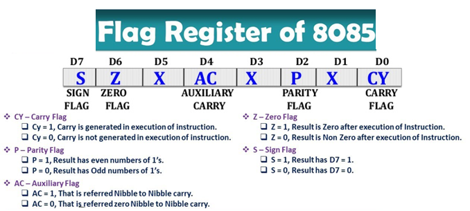
8085 has 5 flags.8086 has 9 flags.8088 has 9 flags.


πŸ˜ƒFor further updates do visit this page regularly.

Thank you all

Images may be subject to copyright

~Pradeep Kumar

Thursday, January 12, 2023

UNIT IV: Memory and I/O Interfacing Questions and Notes

UNIT IV: 

Memory and I/O Interfacing: Minimum and Maximum mode configuration of 8086, Memory Interface with 8086 microprocessor, Address Decoding. Basic I/O Interface: Introduction to I/O Interface, I/O Port Address Decoding. I/O Interface using peripheral devices: The Programmable Peripheral Interface 8255, Programmable Interval Timer 8254. Direct Memory Access: Basic DMA Operation and Definition.

Syllabus Source

https://csvtu.ac.in/ew/download/b-tech-5th-semester-5/?wpdmdl=14364&refresh=63bfa9631ce311673505123

πŸ‘‰Prerequisite:

We have to Learn to do following with 8086.

1. Memory Interfacing 

2. I/O Interfacing

πŸ˜ƒStudy Block Diagram of the Following (SEE CLASS NOTES TO UNDERSTAND  TOPICs) 

i. Minimum and Maximum mode configuration of 8086.

ii. Memory Interface (RAM and EPROM) with 8086.

iii. Programmable Peripheral Interface 8255.

iv. Programmable Interval Timer 8254.

v. Direct Memory Access .

Questions : Compiled from Previous CSVTU Question papers

Topic: Memory Interface (RAM and EPROM) with 8086: 

Needed: Address Mapping and Decoding Circuit

πŸ‘±see class notes


Q. Design an interface between 8086 and two chips of 16K x 8 EPROM (=16KB) and two chips of 32K × 8 RAM (=32KB). Select the starting location of the EPROM suitably. RAM location must start from 00000H. 

Q. Give 8086 Memory Interfacing diagram for 32KB RAM using 16KB RAM and 16KB EPROM using 8KB EPROM, use partial Decoding. 

Q. Interface two 4K X 8 EPROMs and two 4K X 8 RAM chips with 8086 microprocessor. Select Suitable Maps. 

Q. Interface two 8K X 8 EPROMs and four 16K X 8 RAM chips with 8086 microprocessor. The address range is as follows: EPROM 1 & 2: END address is FFFFFH; RAM 1 & 2: Start Address is 10000H; RAM 3 & 4: END address is 1FFFFH. 

Q. Connect a 32kB RAM with the microprocessor 8086 using an absolute decoding with suitable address.

Example problems on memory interfacing with 8086 

(Ref: Advanced Microprocessors and Peripherals by A.K. Ray & K.M. Bhurchandi, 

McGraw-Hill, 2nd Edition.P.158- 164)

πŸ˜„Beyond Syllabus:

if you want to Know how a DYNAMIC RAM  D-RAM 1-T (One Transistor ) based works , see my video:


Topic: I/O Interface with 8086: 

Needed: Block Diagrams 

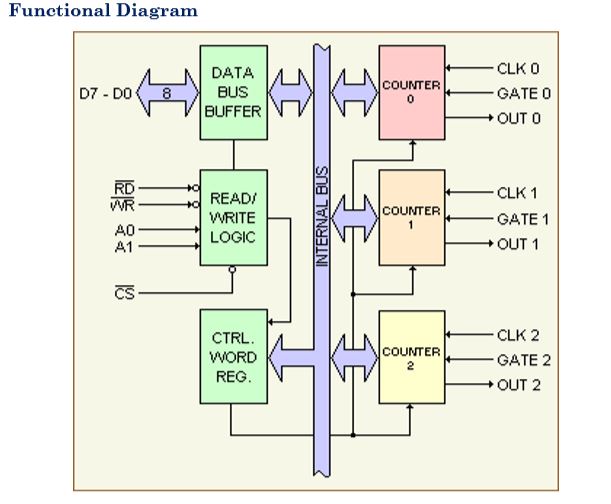
Q. Explain 8254 functional Block Diagram.

Ans: 

PROGRAMMABLE INTERVAL TIMER 8254

The Intel 8254 is a counter/timer device designed to solve the common timing control problems in microcomputer system design. 

8254 is the high speed version of the 8253. 

Application Some of the other counter/timer functions common to microcomputers which can be implemented with the 8254 are: 

 Real time clock 

 Event-counter 

 Digital one-shot 

 Programmable rate generator 

 Square wave generator 

 Binary rate multiplier 

 Complex waveform generator 

 Complex motor controller

 8254 PROGRAMMABLE INTERVAL TIMER functional Block Diagram


It includes Three 16-bit counters COUNTER 0, COUNTER 1, COUNTER3  that can work independently in 6 different modes. 
Modes of Operation 
Mode 0: Interrupt on terminal count. 
Mode 1: Hardware Re triggerable One-Shot. 
Mode 2: Rate Generator. 
Mode 3: Square Wave Mode. 
Mode 4: Software Triggered Mode. 
Mode 5: Hardware Triggered Mode

 It is packaged in a 24-pin DIP(Dual in-line package) and requires +5V power supply. 
 It can count either in binary or BCD. 
 It’s counters can operate at a maximum frequency of 10 MHz's.

Pin functions: 

               A0, A1: The address inputs select one of the four internal registers within the 8254. 

 π‚𝐒: Chip select enables the 8254 for programming and for reading or writing a counter. 
              Vcc: Power connects to the +5V power supply. 
              GND: Ground connects to the system ground bus. 
              GATE : The gate input controls the operation of the counter in some modes of operation. 

               D0-D7: Bidirectional three state data bus lines connected to system data bus. 
 
               CLK : The clock input is the timing source for each of the internal counters. This input is often  connected to the PCLK signal from the microprocessor system bus controller. 


               OUT: A counter output is where the waveform generated by the counter is available. 
 
 
            𝐑𝐃: Read causes data to be read from the 8254 and often connected to the 𝐼𝑂𝑅𝐢 signal. 
            𝐖𝐑: Write causes data to be written to the 8254 and often connects to the write strobe (πΌπ‘‚π‘ŠπΆ) 
Pin.

Programming the 8254 (Control Word Format)

8254 Write operation :
The programming procedure for the 8254 is very flexible. 
Only two conversion need to be remember. 
1) For each Counter, the Control Word must be written before the initial count is written. 
2) The initial count must follow the count format specified in the Control Word (least significant byte only, most significant byte only, or least significant byte and then most significant byte). 

With a clock and an appropriate gate signal to one of the counters, the above steps should start the counter and provide appropriate output according to the control word.

Q. Explain the functional block diagram of 8255 PPI.

Ans:

8255 PPI

8255 PPI (Programmable Peripheral Interface)

It is a programmable peripheral interface, which means it is a programmable device used to interface I/O devices with the processor.

8255 is a programmable I/O device that acts as interface between peripheral devices and the microprocessor for parallel data transfer. 

8255 PPI (programmable peripheral interface) is programmed in a way so as to have transfer of data in different conditions according to the need of the system.


The common applications of 8255 are: 
 

  • Traffic light control
  • Generating square wave
  • Interfacing with DC motors and stepper motors

Architecture of 8255: 

In 8255, 

The three ports are Port A, Port B and Port C and as each port has 8 lines, but the 8 bits of port C is divided into 2 groups of 4-bit each. These are given as port C lower i.e., PC3 – PC0 and port C upper i.e., PC7 – PC4

And are arranged in group of 12 pins each thus designated as Group A and Group B.


Modes of 8255 – It works in two modes: 
 

  1. Bit set reset (BSR) mode.
  2. Input/output (I/O) mode.

I/O mode is further classified into:

Mode 0: Simple input/output
Mode 1: Input output with handshaking

Mode 2: Bidirectional I/O hand shaking

To know in which mode the interface is working we need to know the value of Control word. Control word is a part of control register in 8255 which specify an I/O function for each port. This is format of control word 8255.


Example: 


Q. Explain the Basic DMA operation.

Ans: 

Microprocessor - 8257 DMA Controller

Definition: DMA or Direct Memory Access Controller is an external device that controls the transfer of data between I/O device and memory without the involvement of the processor. It holds the ability to directly access the main memory for read or write operation.

DMA controller was designed by Intel, to have the fastest data transfer rate with less processor utilization.


How DMA Operations are Performed?

Following is the sequence of operations performed by a DMA −

  • 1. Initially, when any device has to send data between the device and the memory, the device has to send DMA request (DRQ) to DMA controller.

  • 2. The DMA controller sends Hold request (HRQ) to the CPU and waits for the CPU to assert the HLDA.

  • 3. Then the microprocessor tri-states all the data bus, address bus, and control bus. The CPU leaves the control over bus and acknowledges the HOLD request through HLDA signal.

  • 4.Now the CPU is in HOLD state and the DMA controller has to manage the operations over buses between the CPU, memory, and I/O devices.

  • 8257:
  • DRQo- DRQ3: These are the four individual channel DMA request inputs, used by the peripheral devices for requesting the DMA services. The DRQo has the highest priority while DRQ3 has the lowest one, if the fixed priority mode is selected. 
  • DACKo- DACK3: These are the active- low DMA acknowledge output lines which inform the requesting peripheral that the request has been honored and the bus is relinquished by the CPU.

Features of 8257

Here is a list of some of the prominent features of 8257 −

  • 1. It has four channels: channel 0, ch1, ch2, ch3 which can be used over four I/O devices.

  • 2. Each channel has 16-bit address and 14-bit counter.

  • 3. Each channel can transfer data up to 64kb.

  • 4. Each channel can be programmed independently.

  • 5. Each channel can perform read transfer, write transfer and verify transfer operations.

  • 6. It operates in 2 modes, i.e., Master mode and Slave mode.

πŸ˜πŸ˜πŸ˜‘πŸ˜’πŸ˜“πŸ˜”πŸ˜•πŸ˜‹πŸ˜ŠπŸ˜‰πŸ˜πŸ˜ž

Thank you all

keep Visiting this page for further updates.

Yours's

Pradeep Kumar


Images may be subject to copyright

Wednesday, January 11, 2023

UNIT V : Advanced Microprocessors: Questions and Notes.

UNIT V: 

Advanced Microprocessors: 80386- Features, block diagram, data types, supported registers, memory system, real mode and protected mode operation, descriptors, cache register, control register, paging mechanism, virtual mode, and protection mechanism for operating system. Comparative Study of Modern Microprocessor (Web based Reference for study): Pentium Pro (Pentium II, Pentium III, Pentium IV), Core i3, i5, i7 and Atom processors.

Syllabus Source:

https://csvtu.ac.in/ew/download/b-tech-5th-semester-5/wpdmdl=14364&refresh=63bfa9631ce311673505123

πŸ‘‰Prerequisite: 

1.Study Features and Architecture / Block Diagram of 80386. (See Class Notes)

πŸ˜ƒWhat to Observe:

i. see process or flow in diagrams from block to block.

ii. see Different Functional Units like BIU, Memory Management Units etc

iii. See the General , Special and Flag Registers.

2. Study Features and Architecture / Block Diagram of Pentium Processor. (See Class Notes).

πŸ˜ƒWhat to Observe:

i. see process or flow in diagrams from block to block.

ii. see 2 ALU's U pipe 32 bit and V Pipe 32 Bit in Execution Unit.


CSVTU asked Questions(Compiled from Previous Year Question Papers)

08 marks or 10 marks Questions : Long Answer Type

1. Explain the internal architecture of 80386 and register organization.

    or

    Draw and explain the block diagram of 80386.

    (πŸ˜ƒDistribution of Marks: 5 Marks for Diagram 5 Marks for Explanation Total 10 Marks)

Ans: Architecture of 80386: 


Register organization of 80386: 

General Registers

The general registers of the 80386 are the 32-bit registers EAX, EBX, ECX, EDX, EBP, ESP, ESI, and EDI. 

Segment Registers

At any given instant, six segments of memory may be immediately accessible to an executing 80386program. The segment registers CS, DS, SS, ES, FS, and GS are used to identify these six current segments.

Flags Register: 

The flags register is a 32-bit register named EFLAGS.


2. Explain the Real mode and Protected mode operation in detail for 80386.

      or

    Explain and compare real, protected and virtual mode operation of 80386 microprocessor.

3. Write the difference between Pentium pro (Pentium II, Pentium III and Pentium IV).

Answer: 

1. The Pentium processor was the first x86 processor with superscalar architecture

2. The Pentium processor also features a 64-bit external data bus, which doubles the amount of information it is possible to read or write on each memory access. 

3. Pentium Pro was introduced in 1995.

The various functional units are as follows:

  1. Bus unit
  2. Paging unit
  3. Control ROM
  4. Prefetch buffer
  5. Execution unit with two integer pipeline (U-pipe and V-pipe)
  6. Code cache
  7. Data cache
  8. Instruction decode
  9. Branch target buffer
  10. Dual processing logic
  11. Advanced programmable interrupt controller

Source: electronics Desk

NOTE: The execution unit within the Pentium microprocessor contains two integer pipelines namely U-pipe and V-pipe and each one has its separate ALU. 

There are five stages in which these pipelines operate, namely, 

prefetch, 

decode-1, 

decode-2, 

execute, 

writeback. 

The U-pipe is responsible for executing all integer as well as floating-point instructions while 

V-pipe executes simple integer and some floating-point instructions.

4. Compare core i3, i5 and i7 and atom processors.

         or

    Write the comparison between Intel Core i3, i5 and i7 under following parameters:

Parameter 

Intel Core i7

Intel Core i5

Intel Core i3

Fabrication process

Technology


Number of Core


Turbo boost

Technology


Size of L2 Cache


Hyper threading

Technology


Number of thread


Power consumption


if above Questions are done we can easily give differences between 8086, 80386, Pentium, i series and Atom Processors.

02 marks Questions: Short Answer Type or Write Short Notes on Following:

1. What are segment descriptors in 80386?

2. What is flag register in 80386.

3. Explain paging mechanism in detail in 80386.


Notes and Other points will keep on updating πŸ’¨πŸ’¬πŸ’­. Visit this blog on regular Basis.

Thank you all

Your's

Pradeep Kumar

Images may be subject to copyright