UNIT IV:
Memory and I/O Interfacing: Minimum and Maximum mode configuration of 8086, Memory Interface with 8086 microprocessor, Address Decoding. Basic I/O Interface: Introduction to I/O Interface, I/O Port Address Decoding. I/O Interface using peripheral devices: The Programmable Peripheral Interface 8255, Programmable Interval Timer 8254. Direct Memory Access: Basic DMA Operation and Definition.
https://csvtu.ac.in/ew/download/b-tech-5th-semester-5/?wpdmdl=14364&refresh=63bfa9631ce311673505123
👉Prerequisite:
We have to Learn to do following with 8086.
1. Memory Interfacing
2. I/O Interfacing
😃Study Block Diagram of the Following (SEE CLASS NOTES TO UNDERSTAND TOPICs)
i. Minimum and Maximum mode configuration of 8086.
ii. Memory Interface (RAM and EPROM) with 8086.
iii. Programmable Peripheral Interface 8255.
iv. Programmable Interval Timer 8254.
v. Direct Memory Access .
Questions : Compiled from Previous CSVTU Question papers
Topic: Memory Interface (RAM and EPROM) with 8086:
Needed: Address Mapping and Decoding Circuit
👱see class notes

Q. Design an interface between 8086 and two chips of 16K x 8 EPROM (=16KB) and two chips of 32K × 8 RAM (=32KB). Select the starting location of the EPROM suitably. RAM location must start from 00000H.
Q. Give 8086 Memory Interfacing diagram for 32KB RAM using 16KB RAM and 16KB EPROM using 8KB EPROM, use partial Decoding.
Q. Interface two 4K X 8 EPROMs and two 4K X 8 RAM chips with 8086 microprocessor. Select Suitable Maps.
Q. Interface two 8K X 8 EPROMs and four 16K X 8 RAM chips with 8086 microprocessor. The address range is as follows: EPROM 1 & 2: END address is FFFFFH; RAM 1 & 2: Start Address is 10000H; RAM 3 & 4: END address is 1FFFFH.
Q. Connect a 32kB RAM with the microprocessor 8086 using an absolute decoding with suitable address.
Example problems on memory interfacing with 8086
(Ref: Advanced Microprocessors and Peripherals by A.K. Ray & K.M. Bhurchandi,
McGraw-Hill, 2nd Edition.P.158- 164)
😄Beyond Syllabus:
if you want to Know how a DYNAMIC RAM D-RAM 1-T (One Transistor ) based works , see my video:
Topic: I/O Interface with 8086:
Needed: Block Diagrams
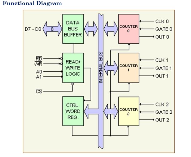
Q. Explain 8254 functional Block Diagram.
Ans:
PROGRAMMABLE INTERVAL TIMER 8254
The Intel 8254 is a counter/timer device designed to solve the common timing control problems in microcomputer system design.
8254 is the high speed version of the 8253.
Application Some of the other counter/timer functions common to microcomputers which can be implemented with the 8254 are:
Real time clock
Event-counter
Digital one-shot
Programmable rate generator
Square wave generator
Binary rate multiplier
Complex waveform generator
Complex motor controller
8254 PROGRAMMABLE INTERVAL TIMER functional Block Diagram:


8254 Write operation :
Q. Explain the functional block diagram of 8255 PPI.
Ans:
8255 PPI
It is a programmable peripheral interface, which means it is a programmable device used to interface I/O devices with the processor.
8255 is a programmable I/O device that acts as interface between peripheral devices and the microprocessor for parallel data transfer.
8255 PPI (programmable peripheral interface) is programmed in a way so as to have transfer of data in different conditions according to the need of the system.

The common applications of 8255 are:
- Traffic light control
- Generating square wave
- Interfacing with DC motors and stepper motors
Architecture of 8255:
In 8255,
The three ports are Port A, Port B and Port C and as each port has 8 lines, but the 8 bits of port C is divided into 2 groups of 4-bit each. These are given as port C lower i.e., PC3 – PC0 and port C upper i.e., PC7 – PC4.
And are arranged in group of 12 pins each thus designated as Group A and Group B.

Modes of 8255 – It works in two modes:
- Bit set reset (BSR) mode.
- Input/output (I/O) mode.
I/O mode is further classified into:
Mode 0: Simple input/outputMode 1: Input output with handshaking
Mode 2: Bidirectional I/O hand shaking
To know in which mode the interface is working we need to know the value of Control word. Control word is a part of control register in 8255 which specify an I/O function for each port. This is format of control word 8255.


Q. Explain the Basic DMA operation.
Ans:
Microprocessor - 8257 DMA Controller
Definition: DMA or Direct Memory Access Controller is an external device that controls the transfer of data between I/O device and memory without the involvement of the processor. It holds the ability to directly access the main memory for read or write operation.
DMA controller was designed by Intel, to have the fastest data transfer rate with less processor utilization.

How DMA Operations are Performed?
Following is the sequence of operations performed by a DMA −
1. Initially, when any device has to send data between the device and the memory, the device has to send DMA request (DRQ) to DMA controller.
2. The DMA controller sends Hold request (HRQ) to the CPU and waits for the CPU to assert the HLDA.
3. Then the microprocessor tri-states all the data bus, address bus, and control bus. The CPU leaves the control over bus and acknowledges the HOLD request through HLDA signal.
4.Now the CPU is in HOLD state and the DMA controller has to manage the operations over buses between the CPU, memory, and I/O devices.

- 8257:
- DRQo- DRQ3: These are the four individual channel DMA request inputs, used by the peripheral devices for requesting the DMA services. The DRQo has the highest priority while DRQ3 has the lowest one, if the fixed priority mode is selected.
- DACKo- DACK3: These are the active- low DMA acknowledge output lines which inform the requesting peripheral that the request has been honored and the bus is relinquished by the CPU.

Features of 8257
Here is a list of some of the prominent features of 8257 −
1. It has four channels: channel 0, ch1, ch2, ch3 which can be used over four I/O devices.
2. Each channel has 16-bit address and 14-bit counter.
3. Each channel can transfer data up to 64kb.
4. Each channel can be programmed independently.
5. Each channel can perform read transfer, write transfer and verify transfer operations.
6. It operates in 2 modes, i.e., Master mode and Slave mode.
😏😐😑😒😓😔😕😋😊😉😝😞
Thank you all
keep Visiting this page for further updates.
Yours's
Pradeep Kumar
Images may be subject to copyright
No comments:
Post a Comment