Monday, May 22, 2023

CSA UNIT 3 MEMORY SYSTEMS

CSA  # UNIT 3 : MEMORY SYSTEMS


MEMORY SYSTEMS: 
๐Ÿ‘ตPrerequisite: Go through the notes below before Answering the Questions

The memory hierarchy system consists of all storage devices contained in a computer system from the slow Auxiliary Memory to fast Main Memory and to smaller Cache memory

Auxiliary memory access time is generally 1000 times that of the main memory, hence it is at the bottom of the hierarchy.


The Goal:๐Ÿ‘จ illusion of large, fast, cheap memory

 • Fact: Large memories are slow, fast memories are small

 • How do we create a memory that is large, cheap and fast (most of the time)?

 – Hierarchy

 – Parallelism 

so, 

 – Present the user with as much memory as is available in the cheapest technology.

 – Provide access at the speed offered by the fastest technology. 


How is the hierarchy managed?

 • Registers <-------> Memory – by compiler (programmer?)

 • cache <-------> memory – by the hardware

 • memory <--------> disks – by the hardware and operating system (virtual memory) – by the programmer (files)

 • Virtual memory – Virtual layer between application address space to physical memory – Not part of the physical memory hierarchy 


Memory Technology

 *Random Access: – "Random" is good: access time is the same for all locations

 – DRAM: Dynamic Random Access Memory

 • High density, low power, cheap, slow

 • Dynamic: need to be refreshed regularly

  • Main Memory is DRAM 


See My Lecture/ VIDEO : Click ๐Ÿ‘‰๐ŸŽฌ or Directly click on the Video below:


 – SRAM: Static Random Access Memory

 • Cache uses SRAM : Static Random Access Memory – No refresh

• Low density, high power, expensive, fast

 • Static: content will last forever (until lose power)

Example: 


 * "Non-so-random" Access Technology: – Access time varies from location to location and from time to time

 – Examples: Disk, CDROM

  * Sequential Access Technology: access time linear in location (e.g., Tape) 

So,

•  DRAM is slow but cheap and dense: – Good choice for presenting the user with a BIG memory system

 • SRAM is fast but expensive and not very dense: – Good choice for providing the user FAST access time.  

Increasing Bandwidth - Interleaving  : Refer Question#

Disk Storage

• Nonvolatile, rotating magnetic storage:


Magnetic Disks

  • Traditional magnetic disks have the following basic structure:
    • One or more platters in the form of disks covered with magnetic media. Hard disk platters are made of rigid metal, while "floppy" disks are made of more flexible plastic.
    • Each platter has two working surfaces. Older hard disk drives would sometimes not use the very top or bottom surface of a stack of platters, as these surfaces were more susceptible to potential damage.
    • Each working surface is divided into a number of concentric rings called tracks. The collection of all tracks that are the same distance from the edge of the platter, ( i.e. all tracks immediately above one another in the following diagram ) is called a cylinder.
    • Each track is further divided into sectors, traditionally containing 512 bytes of data each, although some modern disks occasionally use larger sector sizes. ( Sectors also include a header and a trailer, including checksum information among other things. Larger sector sizes reduce the fraction of the disk consumed by headers and trailers, but increase internal fragmentation and the amount of disk that must be marked bad in the case of errors. )
    • The data on a hard drive is read by read-write heads. The standard configuration ( shown below ) uses one head per surface, each on a separate arm, and controlled by a common arm assembly which moves all heads simultaneously from one cylinder to another. ( Other configurations, including independent read-write heads, may speed up disk access, but involve serious technical difficulties. )
    • The storage capacity of a traditional disk drive is equal to the number of heads ( i.e. the number of working surfaces ), times the number of tracks per surface, times the number of sectors per track, times the number of bytes per sector. A particular physical block of data is specified by providing the head-sector-cylinder number at which it is located.

****************************************************

Questions and Answers ( As per previous year CSVTU QP): 

1. Explain Memory Hierarchy , give details of each levels in brief.

Ans: 


Levels of memory: 

• Level 0 or Register – It is a type of memory in which data is stored and accepted that are immediately stored in CPU. Most commonly used register is accumulator, Program counter, address register etc. 

• Level 1 or Cache memory – It is the fastest memory which has faster access time where data is temporarily stored for faster access. 

• Level 2 or Main Memory – It is memory on which computer works currently. It is small in size and once power is off data no longer stays in this memory. 

• Level 3 or Secondary Memory – It is external memory which is not as fast as main memory but data stays permanently in this memory.


2. What is Virtual memory in Computer System? Give Details of Paging Mechanism. How it is different from Main memory.

Ans: See my Class notes: Click๐Ÿ‘‰ Paging Mechanism

OR

Virtual memory is a memory management technique where secondary memory can be used as if it were a part of the main memory.

Virtual memory is a valuable concept in computer architecture that allows you to run large, sophisticated programs on a computer even if it has a relatively small amount of RAM. A computer with virtual memory artfully juggles the conflicting demands of multiple programs within a fixed amount of physical memory.

Virtual memory is a common technique used in a computer's operating system (OS). 

How does virtual storage work?

This memory system uses both the computer's software and hardware to work. It transfers processes between the computer's RAM and hard disk by copying any files from RAM that aren't currently in use and moving them to the hard disk. 

Virtual storage management: 

Computers can handle virtual storage through segmenting and paging. Below is an explanation of the Paging Mechanism.


Paging Mechanism:

Paging is a Memory management method.

The process of retrieving processes in the form of pages from the secondary storage into the main memory is known as paging.

In paging, the physical memory is divided into fixed-size blocks called page frames, which are the same size as the pages used by the process. The process’s logical address space is also divided into fixed-size blocks called pages, which are the same size as the page frames. 

Now we usually divide the Main Memory in to Frames of equal sizes. And in return each of the Frame consists of equal number of words.

Important Point to be noted is that Page Size = Frame Size.
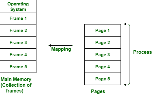

Let us assume 2 processes, P1 and P2, contains 4 pages each. Each page size is 1 KB. The main memory contains 8 frame of 1 KB each. The OS resides in the first two partitions. In the third partition, 1st page of P1 is stored and the other frames are also shown as filled with the different pages of processes in the main memory.

The page tables of both the pages are 1 KB size each and therefore they can be fit in one frame each. The page tables of both the processes contain various information that is also shown in the image.

The CPU contains a register which contains the base address of page table that is 5 in the case of P1 and 7 in the case of P2. This page table base address will be added to the page number of the Logical address when it comes to accessing the actual corresponding entry.


A Translation look aside buffer can be defined as a memory cache which can be used to reduce the time taken to access the page table again and again.

It is a memory cache which is closer to the CPU and the time taken by CPU to access TLB is lesser then that taken to access main memory.


3. A Two way Set Associative Cache Memory uses a Block of Size 128 bytes with Total Cache Size 1MB. Byte . Addressable Main Memory Size is given as 256 MB.

Give the Physical Address Splits in bits.

Ans: See my Class notes : 

         click ๐Ÿ‘‰ Types of Cache mapping Theory with Solved Numerical

or


First lets see the theory behind it: 

In OS we have two kind of addresses: 

Virtual/Logical Address, and Physical Address.

Physical Address:
As explained above that CPU generates addresses of all the processes in the main memory relative to zero i.e., CPU produces address starting from 0.Now the addresses generated by are no way real because if those addresses were valid then all processes would begin from zero and rest spaces in Main Memory would be memory. Thus the addresses generated by CPU should be some way mapped to real (physical address) of the Main Memory. This is done by MMU (Memory Management unit).

he smallest addressable unit in memory is called word. It means the smallest unit which can specifically identified using address bits.

The Address Space of Virtual Address is divided into 2 parts: Page Number, and Page OFFset.

Similarly, the Address Space of Physical Address is divided into 2 parts: Frame Number, and Frame OFFset.

Let Virtual Address has n bits and Physical Address has m bits.

Page Size = Frame Size = k bits 

(as page size = Frame size as mentioned above).

Number of Pages = 2(n-k) pages
Number of Frames = 2(m-k) Frames


5. Give all Information required to construct Cache Memory. 

Ans: 

    Cache Memory

    Cache Memory is a special very high-speed memory. It is used to speed up and synchronizing with high-speed CPU.

    Cache Performance: 

    When the processor needs to read or write a location in main memory, it first checks for a corresponding entry in the cache. 

    • If the processor finds that the memory location is in the cache, a cache hit has occurred and data is read from cache 

    • If the processor does not find the memory location in the cache, a cache miss has occurred. For a cache miss, the cache allocates a new entry and copies in data from main memory, then the request is fulfilled from the contents of the cache. 

    The performance of cache memory is frequently measured in terms of a quantity called Hit ratio.

    Hit ratio = hit / (hit + miss) =  no. of hits/total accesses

    Cache Mapping:

      There are three different types of mapping used for the purpose of cache memory which is as follows: Direct mapping, Associative mapping, and Set-Associative mapping.
    1. Direct Mapping –
      Maps each block of main memory into only one possible cache line. If a line is previously taken up by a memory block and a new block needs to be loaded, the old block is trashed. An address space is split into two parts index field and a tag field. The cache is used to store the tag field whereas the rest is stored in the main memory.
    2. Associative Mapping –
      A block of main memory can map to any line of the cache that is freely available at that moment. The word offset bits are used to identify which word in the block is needed, all of the remaining bits become Tag.
    3. Set-Associative Mapping –
      Cache lines are grouped into sets where each set contains k number of lines and a particular block of main memory can map to only one particular set of the cache. However, within that set, the memory block can map to any freely available cache line.

Note: Translation Lookaside Buffer (i.e. TLB) is required only if Virtual Memory is used by a processor. In short, TLB speeds up the translation of virtual address to a physical address by storing page-table in faster memory. In fact, TLB also sits between the CPU and Main memory.


What is Direct Mapping? 

(source:https://byjus.com/gate/direct-mapping-notes/)

In the case of direct mapping, a certain block of main memory would be able to map to only a particular line of cache.

Physical Address Division

The physical address, in the case of direct mapping, is divided as follows:


What is Fully Associative Mapping?

“Every memory block can be mapped to any cache line.”

The fully associative mapping helps us resolve the issue related to conflict misses. It means that any block of the main memory can easily come in a line of cache memory. Here, for instance, B0 can easily come in L1, L2, L3, and L4. Also, the case would be similar for all the other blocks. This way, the chances of a cache hit increase a lot.

Now, let us assume that there is a RAM (Main Memory) size of 128 Words along with a Cache size of 16 Words. Here, the Cache and the Main Memory are divided into Lines and blocks, respectively. Every block Line is of the size 4- words. It is shown in the diagram given as follows:


Physical Address

Since the main memory has a size of 128 words, a total of 7 bits would be used for representing the main memory. Thus, the Physical address would be 7 bits in size. Given below is an example of the fully associative mapping of W24 of the B6.


What is K-way Set Associative Mapping?

The K-way set associative mapping is like a mix of fully associative and direct mapping. Here,

  • The total number of sets = The total number of lines/K
  • K refers to the K-way set associative
  • K= 23 for a 2-way set associative
  • The total number of sets = 4/2 or 2 sets (S1, S0)


Physical Address

In case a cache has 4 lines, and we consider a 2-way set associative, then:

6. What is Memory Interleaving?

Ans:

 See my Class notes : click ๐Ÿ‘‰ Memory Interleaving

or

Prerequisite – see Q#2.

Abstraction is one of the most important aspects of computing. It is a widely implemented Practice in the Computational field. 

Memory Interleaving is less or More an Abstraction technique. Though it’s a bit different from Abstraction. 

It is a Technique that divides memory into a number of modules such that Successive words in the address space are placed in the Different modules. 


***************************************************************************


Thank you all


~pradeep


---------------------------------------------------------------------------------------------------------------------
Disclaimer:  เคธाเค‡เคŸ เคชเคฐ เคธाเคฎเค—्เคฐी เค•ेเคตเคฒ เคถैเค•्เคทिเค• เค‰เคฆ्เคฆेเคถ्เคฏों เค•े เคฒिเค เคนै เค”เคฐ เคฏเคน เคชेเคถेเคตเคฐ เคธเคฒाเคน เคจเคนीं เคนै।

Educational Purpose Only: The information provided on this blog is for general informational and educational purposes only. All content, including text, graphics, images, and other material contained on this blog, is intended to be a resource for learning and should not be considered as professional advice.

No Professional Advice: The content on this blog does not constitute professional advice, and you should not rely on it as a substitute for professional consultation, diagnosis, or treatment. Always seek the advice of a qualified professional with any questions you may have regarding a specific issue.

Accuracy of Information: While I strive to provide accurate and up-to-date information, I make no representations or warranties of any kind, express or implied, about the completeness, accuracy, reliability, suitability, or availability with respect to the blog or the information, products, services, or related graphics contained on the blog for any purpose. Any reliance you place on such information is therefore strictly at your own risk.

External Links: This blog may contain links to external websites that are not provided or maintained by or in any way affiliated with me. Please note that I do not guarantee the accuracy, relevance, timeliness, or completeness of any information on these external websites.

Personal Responsibility: Readers of this blog are encouraged to do their own research and consult with a professional before making any decisions based on the information provided. I am not responsible for any loss, injury, or damage that may result from the use of the information contained on this blog.

Contact: If you have any questions or concerns regarding this disclaimer, please feel free to contact me at my email: pradeep14335@gmail.com

CSA UNIT 2 ARITHEMATIC

CSA UNIT 2 # ARITHEMATIC


Questions and Answers (as per previous year CSVTU QP): 

1. Explain the working of 4 bit Fast Adder Carry Look Ahead Adder with neat Diagram.

Ans:  see class notes : Click ๐Ÿ‘‰ Lookahead carry adder

OR

What is a Carry Look-ahead Adder?

A digital computer must contain circuits which can perform arithmetic operations such as addition, subtraction, multiplication, and division. Among these, addition and subtraction are the basic operations whereas multiplication and division are the repeated addition and subtraction respectively.

To perform these operations ‘Adder circuits’ are implemented using basic logic gates. Adder circuits are evolved as Half-adder, Full-adder, Ripple-carry Adder, and Carry Look-ahead Adder.


2. Give the Flow table for the register’s Content used in implementing above Algorithm.

Ans : For Algorithm and Flowchart , Click ๐Ÿ‘‰ Booth's Algorithm

OR

The booth algorithm is a multiplication algorithm that allows us to multiply the two signed binary integers in 2's complement, respectively. It is also used to speed up the performance of the multiplication process. It is very efficient too.

Working on the Booth Algorithm

  1. Set the Multiplicand and Multiplier binary bits as M and Q, respectively.
  2. Initially, we set the AC and Qn + 1 registers value to 0.
  3. SC represents the number of Multiplier bits (Q), and it is a sequence counter that is continuously decremented till equal to the number of bits (n) or reached to 0.
  4. A Qn represents the last bit of the Q, and the Qn+1 shows the incremented bit of Qn by 1.
  5. On each cycle of the booth algorithm, Qn and Qn + 1 bits will be checked on the following parameters as follows:
    1. When two bits Qn and Qn + 1 are 00 or 11, we simply perform the arithmetic shift right operation (ashr) to the partial product AC. And the bits of Qn and Qn + 1 is incremented by 1 bit.
    2. If the bits of Qn and Qn + 1 is shows to 01, the multiplicand bits (M) will be added to the AC (Accumulator register). After that, we perform the right shift operation to the AC and QR bits by 1.
    3. If the bits of Qn and Qn + 1 is shows to 10, the multiplicand bits (M) will be subtracted from the AC (Accumulator register). After that, we perform the right shift operation to the AC and QR bits by 1.
  6. The operation continuously works till we reached n - 1 bit in the booth algorithm.
  7. Results of the Multiplication binary bits will be stored in the AC and QR registers.


3Multiply (+5) and (-7) using Booth’s Algorithm. 

Ans: Click ๐Ÿ‘‰ 5 * -7

4. Multiply (+5) and (+7) using Booth’s Algorithm.

Ans: Click ๐Ÿ‘‰ +5 * +7

5. Explain the circuit for Binary Parellel Adder/Subtractor circuit using full Adder.

Ans: Click ๐Ÿ‘‰Adder cum Subtractor circuit


Tuesday, March 21, 2023

UNIT 1 - Basic Structures of Computers (CSVTU, BHILAI: COMPUTER SYSTEM ARCHITECTURE NOTES) :

Branch: CSE/AI/AI&DS/AI&ML

Syllabus : Refer CSVTU website
click here 


UNIT 1 - Basic Structures of Computers:
Syllabus: 

Notes:   (Go through these points before answering the Questions)
๐Ÿ‘ฆPrerequisite – 
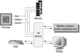
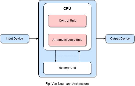
Systems architecture refers to the structure of the internal components of a computer system. Modern computers often have a von Neumann architecture, which involves: a processor; a memory unit, which stores both instructions and data; connections for input and output devices; and secondary storage for data.


Block Diagram of the computer.


In the 1940s, John von Neumann and his team developed the concept of the stored program computer.
John von Neumann coined and developed this architecture. The computer we are using nowadays is based on the von Neumann architecture. It is also known as Princeton architecture.


Harvard Architecture consists of code and data laid in distinct memory sections. It requires a separate memory block for data and instruction.

In a system or computer, most of the tasks are controlled with the help of a processor or CPU (Central processing unit), which is the main component of a computer. 

The CPU usually has two main systems: control unit (CU) and arithmetic and logic unit (ALU). 

The control unit (CU) is used to synchronize the tasks with the help of sending timings and control signals. On the other hand, mathematical and logical operations can be handled with the help of ALU. 

Micro programmed control units and hardwired control units can be called two types of control units. 

We can execute an instruction with the help of these two control units.

In the hardwired control unit, the execution of operations is much faster, but the implementation, modification, and decoding are difficult. In contrast, implementing, modifying, decoding micro-programmed control units is very easy. The micro-programmed control unit is also able to handle complex instructions. With the help of control signals generated by micro-programmed and hardwired control units, we are able to fetch and execute the instructions.

Figure – Basic CPU structure๐Ÿ‘‡


Instruction Formats (Zero, One, Two and Three Address Instruction)

A instruction is of various length depending upon the number of addresses it contain. Generally CPU organization are of three types on the basis of number of address fields:

  1. Single Accumulator organization
  2. General register organization
  3. Stack organization
  1. Zero Address Instructions –
    Address is stored in the opcode, in the zero address instruction. A stack based organization uses zero address instruction.
  2. One Address Instructions –
    This use a implied ACCUMULATOR register for data manipulation. One operand is in accumulator and other is in register or memory location. Implied means that the CPU already know that one operand is in accumulator so there is no need to specify it. i.e there will be one opcode field and one address field.
  3. Two Address Instructions –
    Here two address can be specified in the instruction. Unlike earlier in one address instruction, the result was stored in accumulator here result can be stored at a different location rather than just accumulator, but require the number more of the bit to represent address.
  4. Three Address Instructions –
    This has three address field to specify a register or a memory location. The program created is much short in size but the number of bits per instruction increase.

Addressing Modes

The term addressing modes refers to the way in which the operand of an instruction is specified. The addressing mode specifies a rule for interpreting or modifying the address field of the instruction before the operand is actually executed.

An assembly language program instruction consists of two parts


Refer Q#4 For more details.


๐Ÿ‘ฆPrerequisite – 

There are two approaches of the design of the control unit of a microprocessor i.e.-

  • Hardware approach. &
  • Software approach.
Study ๐Ÿ‘‰ Hardwired and Micro Programmed Control Unit.
To execute an instruction, there are two types of control units Hardwired Control unit and Micro-programmed control unit.

Question and Answers : (As per previous year CSVTU QP)

1. Explain the working of Hardwired Control Unit with neat Block Diagram.

Ans: See detailed Notes: 

๐Ÿ‘งAll 3 methods including Sequence Counter method

      click๐Ÿ‘‰ 3 methods of hard wired Control Units

 ๐Ÿ‘ดFor Sequence Counter method: 

      click๐Ÿ‘‰sequence counter method hard wired CU

or 

Designing methods of hardwired control unit

Here the control signals are generated using hardware.   
There are three types of Hardwired Control Units.
1State table method :

  • Here the behavior of control unit is represented in the form of a table, which is known as the state table.
  • Here, each row represents the T-states and the columns represent the instructions.
  • Every intersection of the specific column to each row indicates which control signal will be produced in the corresponding T- state of an instruction.
  • Here the hardware circuitry is designed for each column(i.e. for a specific instruction) for producing control signals in different T-states.

2. Delay element method :

  • Here the control unit behavior is represented in the form of a flowchart.
  • Each step in the flowchart represents a control signal that needs to be produced for processing the instructions.
  • If all the steps of the instructions are performed, this means the instruction is executed completely.
  • Control signals perform micro-operations and each micro-operation requires one T-state.
  • For the micro-operations which are independent, they are required to be performed in different T-state. Therefore, for every consecutive control signal an exactly 1-state delay is required, which can be produced with the help of D FF.
  • Therefore. D Flip-Flops are inserted between every two consecutive control signals.


3. Sequence counter method :
This is the most popular and most commonly used method for generating delays between every consecutive control signal. 
It is similar to the delay element method, but the only difference is that instead of unnecessary D Flip flops there are triggering points in the circuit. They are activated after a gap of one-one  T-state.

Working of Sequence counter circuit –

  • Here one SR FF , one decode and one counter is used.
  • When the instruction cycle starts, then start = 1.
  • As we know, when Start =  1, because S is connected to Start, therefore Q  becomes 1 and and Q’ becomes 0.
  • Here the level triggering clock is used. Therefore, when clock = 1 or high and Start=1, as both outputs are connected to AND gate, so if the resultant of both is 1 that will enable the counter and counter starts counting from 0 0 0 state. So the 0 0 0 state is decoded by a decoder and produces output O1 , which will trigger the triggering point in the control circuit.
  • Suppose the counter is 3 bits, it generates 23 = 8 states(000 001 ….. 111) . The first count 0 0 0 is given to 3:8 decoder. It will active output number 1. This output is not a control signal but this will trigger the triggering point in the control unit circuit.
  • As the clock becomes high again after a gap of one T state, therefore clock =1 and start = 1 ,then the counter is enabled and changes it state to 001 and the counter decodes the count and makes O2 output high . And this will trigger a second triggering point in the circuit.
  • All counting states are decoded in the same manner.
2. Explain the working of Micro Programmed Control Unit with neat Block Diagram.

Ans:

See detailed Notes: 

Wilke's Design: click๐Ÿ‘‰  Wilke's design

Some Drawbacks are there in Wilke's design, modified Diagram is shown below๐Ÿ‘‡

Modern Approach : Modification of Wilke's Design : Modern Approach Microprogrammed Control Unit

or
The microprogrammed control unit uses the software approach to generate the control signals. The generation of the control signals is determined with the help of the program. This program is stored in the special memory of the processor which is smaller and faster. This memory is termed as microprogram memory or control store and the program is termed as the microprogram.

Microprogrammed Control Unit :
Microprogrammed Control Unit produces control signals by using micro-instructions.

Micro program :

  • A program is a set of instructions. An instruction requires a set of micro-operations.
  • Micro-operations are performed using control signals.
  • Here, these control signals are generated using micro-instructions.
  • This means every instruction requires a set of micro-instructions
  • A set of micro-instructions are called micro-program.
  • Microprograms for all instructions are stored in a small memory called control memory. 
    The control memory is present inside the processor.

Working : 
Consider an instruction that is fetched from the main memory into the instruction Register (IR). 

The processor uses its unique opcode to identify the address of the first micro-instruction. 

That address is loaded into CMAR (Control Memory Address Register). 

This address is decoded to decide the corresponding memory instruction from the control Memory. 

Micro-instructions will only have a control field. The control field Indicates the control signals to be generated. Most micro-instructions will not have an address field. 

Usually ยตPC will simply get incremented after every micro-instruction. 


This is as long as the micro-program is executing sequentially. 

If there is a branch micro-instruction only then there will be an address filed. 

If the branch is unconditional, the branch address will be directly loaded into CMAR.

For conditional branches, the branch condition will check the appropriate flag. This is done using a MUX which has all flag inputs. If the condition is true, then the mux will inform CMAR to load the branch address. If the condition is false CMAR will simply get incremented.
The control memory is usually implemented using flash ROM as it is non-volatile.


3. Write the Differences between Hardwired and Micro Programmed Control Unit.
Ans: ๐Ÿ‘ฆPrerequisite – See Q#1 for details

Difference Chart

Basis of DifferentiationHardwired Control UnitMicroprogrammed Control Unit
BasicIt is a circuitry approach.This control unit is implemented by programming
DesignRISC style instructionsCISC style instructions
ModificationModification is difficult as the control unit is hardwired. Modifying it will require the change in hardware.Modifications are easy in case of microprogrammed control unit as it will require the in change in the code only.
InstructionsIt works well for simple instructions.It works well for complex instructions also.
CostingImplementing hardwired structure requires a cost.Implementing microprograms is not costly.
Control memoryNo control memory is requiredControl memory is required
Execution SpeedFaster execution

Comparatively slow
4. What are Addressing Modes? Explain various Addressing modes with an Example.
Ans: 
The instruction set of a microprocessor is a list of all the software instructions that the processor can execute.When an instruction expressed in machine code, it is encoding using 0’s and 1’s(in hexadecimal format)

Types of addressing mode in Intel Microprocessor 8086

  1. Immediate addressing modeMOV AX,10ABH
  2. Direct addressing mode: MOV AX, [5000H]
  3. Register addressing mode: MOV AX,BX
  4. Register Indirect addressing mode: MOV AX,[BX]
  5. Indexed addressing mode: MOV AX,[SI]
  6. Register relative addressing mode: MOV AX, 50H[BX]
  7. Base plus index addressing mode: MOV AX, [BX] [SI]
  8. Base relative plus index addressing mode: MOV AX,50H[BX][SI]

Detailed Explanation: 


Note: An instruction may have 0-3 number of operands


Types of addressing modes:

  1. Register mode – In this type of addressing mode both the operands are registers.
    Example:
    MOV AX, BX
    XOR AX, DX
    ADD AL, BL
  2. Immediate mode – In this type of addressing mode the source operand is a 8 bit or 16 bit data. Destination operand can never be immediate data.
    Example:
    MOV CL, 0A
    ADD AL, 45
  3. Displacement or direct mode – In this type of addressing mode the effective address is directly given in the instruction as displacement, Example: MOV AX, [DISP]; MOV AX, [0500]
  4. Register indirect mode – In this addressing mode the effective address is in SI, DI or BX. Example: Physical Address = Segment Address + Effective Address, MOV AX, [DI]; ADD AL, [BX]; MOV AX, [SI] 
  5. Based indexed mode – In this the effective address is sum of base register and index register. Base register: BX, BP; Index register: SI, DI
  6. Indexed mode – In this type of addressing mode the effective address is sum of index register and displacement.
    Example:
    MOV AX, [SI+2000]
    MOV AL, [DI+3000]
  7. Based mode – In this the effective address is the sum of base register and displacement.
    Example:
    MOV AL, [BP+ 0100]
  8. Based indexed displacement mode – In this type of addressing mode the effective address is the sum of index register, base register and displacement.
    Example:
    MOV AL, [SI+BP+2000]

5. An instruction is stored at location 300 with its address field at location 301. The address field has the value 400, a processor register R1 contain the number 200. Evaluate Effective address if the addressing mode of the instruction are

(i) Direct

(ii) Immediate

(iii) Register Indirect

(iv) 
Relative
(v) Indexed

Answer:

the effective address if the addressing mode of the instruction is (i) 400 (ii) 301 (iii) 200 (iv)701 (v) 600


Explanation:

Given: An instruction is stored at location 300 with its address field at location 301. The address field at location 301. The address field has the value 400. A processor register r1 contains the number 200.


To find:  Evaluate the effective address if the addressing mode of the instruction is (i) direct (ii) immediate (iii) register indirect  (iv)relative (v) index with r1 as the index register

Solution: Note: An effective address is any operand to an instruction which references memory

The description given in the assignment can be represented like this:

Location _ Contents

300 _ opcode ; the instruction operation code

301 _ 400 ; address field of the above instruction

(a) Direct Addressing

(Example: Direct addressing mode: MOV AX, [5000H] means the content at memory location 5000 will be copied to AX), so as per our question,

Direct addressing means that the address field contains the address of memory location the instruction is supposed to work with (where an operand "resides").

Effective address would therefore be 400.

(b) immediate addressing:

(Example: Immediate addressing modeMOV AX,10AB)H

Immediate addressing means that the address field contains the operand itself.

Effective address would therefore be 301.

(c) register indirect addressing: 

(Ex: Register Indirect addressing mode: MOV AX,[BX])

Register indirect addressing means that the address of an operand is in the register. The address field in this case contains just another operand.

Effective address would therefore be in R1 = 200.

(d) relative addressing

(Ex: Register relative addressing mode: MOV AX, 50H[BX])

Relative addressing means that the address field contains offset to be added to the program counter to address a memory location of the operand.

Effective address would therefore be 301 + 400 = 701.

(e) indexed addressing with R1 as index register

There are several possible indexed addressing modes but in this case (there is an address field) it is co called "indexed absolute" addressing.

In indexed absolute addressing the effective address is calculated by taking the contents of the address field and adding the contents of the index register.

Effective address would therefore be 400 + R1 = 400 + 200 = 600.


6. What are the various Buses types in Computer system.
Ans: 
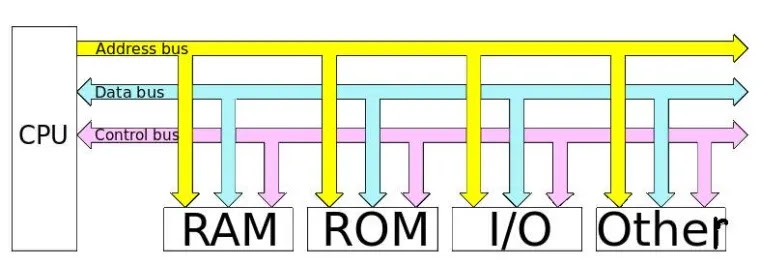
Inside computers, there are many internal components. In order for these components to communicate with each other, they make use of wires that are known as a ‘bus’.
There are three types of bus lines: Data bus, Address bus, and Control bus.

The address bus, which is a unidirectional pathway that allows information to travel in only one direction, carries information about where data will be stored in memory.

The data bus is a bidirectional pathway that carries the actual data (information) to and from the main memory.

The control bus carries the control and timing signals needed to coordinate the activities of the entire computer. Think of this as a traffic cop.


Pic Source: The Computer Buses Wikimedia Commons


Bus TypeDescription
Address busA unidirectional pathway – information can only flow one way
Data busA bi-directional pathway – information can flow in two directions
Control busCarries the control and timing signals needed to coordinate the activities of the entire computer
7. Explain Microoperations
or
Explain Instruction Execution
or
Explain significance of MAR, MBR , IR, GPR in execution of microoperations for fetching an Instruction.
Ans: See detailed Notes:  click๐Ÿ‘‰ Microoperation 

OR ๐Ÿ‘ฒSee the notes below: 


    Microprogram: Program stored in memory that generates all control signals required to execute the instruction set correctly, it consists micro-instructions.
    Micro-instruction: Contains a sequencing word and a control word. The control word is all control information required for one clock cycle.
    Micro-operations: Micro-operations are the atomic operations which executes a particular micro-instruction.
    Example of micro-operation during the fetch cycle:

    t1: MAR ←(PC)
    t2: MBR ←Memory
        PC ←(PC) + 1
    t3: IR ←(MBR)

  • Things a CPU must do:
    • Fetch Instructions
    • Interpret Instructions
    • Fetch Data
    • Process Data
    • Write Data
  • Components of the CPU
    • Arithmetic and Logic Unit (ALU): does the actual computation or processing of data
    • Control Unit (CU): controls the movement of data and instructions into and out of the CPU and controls the operation of the ALU.
  • A small amount of internal memory, called the registers, is needed by the CPU to fulfill these requirements


Register Organization

  • Registers are at top of the memory They serve two functions:
  1. User-Visible Registers - enable the machine- or assembly-language programmer to minimize main-memory references by optimizing use of registers
  2. Control and Status Registers - used by the control unit to control the operation

User-Visible Registers

Categories of Use

  • General Purpose registers - for variety of functions
  • Data registers - hold data
  • Address registers - hold address information
  • Segment pointers - hold base address of the segment in use
  • Index registers - used for indexed addressing and may be auto indexed
  • Stack Pointer - a dedicated register that points to top of a Push, pop, and other stack instructions need not contain an explicit stack operand.

Control and Status Registers

  • Essential to instruction execution
    • Program Counter (PC)
    • Instruction Register (IR)
    • Memory Address Register (MAR) - usually connected directly to address lines of bus
    • Memory Buffer Register (MBR) - usually connected directly to data lines of bus
  • Program Status Word (PSW) - also essential, common fields or flags contained include:
    • Sign - sign bit of last arithmetic operation
    • Zero - set when result of last arithmetic operation is 0
    • Carry - set if last op resulted in a carry into or borrow out of a high-order bit
    • Equal - set if a logical compare result is equality
    • Overflow - set when last arithmetic operation caused overflow
    • Interrupt Enable/Disable - used to enable or disable interrupts

The Instruction Cycle

    Instruction Cycle

    Registers Involved In Each Instruction Cycle:

    • Memory address registers(MAR) : It is connected to the address lines of the system bus. It specifies the address in memory for a read or write operation.
    • Memory Buffer Register(MBR) : It is connected to the data lines of the system bus. It contains the value to be stored in memory or the last value read from the memory.
    • Program Counter(PC) : Holds the address of the next instruction to be fetched.
    • Instruction Register(IR) : Holds the last instruction fetched.

Basic instruction cycle contains the following sub-cycles.

  • Fetch - read next instruction from memory into CPU
  • Execute - Interpret the opcode and perform the indicated operation
  • Interrupt - if interrupts are enabled and one has occurred, save the current process state and service the interrupt


Data Flow

  • Exact sequence depends on CPU design
  • We can indicate sequence in general terms, assuming CPU employs:
    • a memory address register (MAR)
    • a memory buffer register (MBR)
    • a program counter (PC)
    • an instruction register (IR)

Fetch cycle data flow

  • PC contains address of next instruction to be fetched
  • This address is moved to MAR and placed on address bus
  • Control unit requests a memory read
  • Result is
    • placed on data bus
    • result copied to MBR
    • then moved to IR

Meanwhile, PC is incremented.


************************************************************************************

for any further queries and doubts in this subject
please feel to write to me or contact me at:
Pradeep Kumar Chaudhary
pradeep14335@gmail.com


---------------------------------------------------------------------------------------------------------------------
Disclaimer:  เคธाเค‡เคŸ เคชเคฐ เคธाเคฎเค—्เคฐी เค•ेเคตเคฒ เคถैเค•्เคทिเค• เค‰เคฆ्เคฆेเคถ्เคฏों เค•े เคฒिเค เคนै เค”เคฐ เคฏเคน เคชेเคถेเคตเคฐ เคธเคฒाเคน เคจเคนीं เคนै।

Educational Purpose Only: The information provided on this blog is for general informational and educational purposes only. All content, including text, graphics, images, and other material contained on this blog, is intended to be a resource for learning and should not be considered as professional advice.

No Professional Advice: The content on this blog does not constitute professional advice, and you should not rely on it as a substitute for professional consultation, diagnosis, or treatment. Always seek the advice of a qualified professional with any questions you may have regarding a specific issue.

Accuracy of Information: While I strive to provide accurate and up-to-date information, I make no representations or warranties of any kind, express or implied, about the completeness, accuracy, reliability, suitability, or availability with respect to the blog or the information, products, services, or related graphics contained on the blog for any purpose. Any reliance you place on such information is therefore strictly at your own risk.

External Links: This blog may contain links to external websites that are not provided or maintained by or in any way affiliated with me. Please note that I do not guarantee the accuracy, relevance, timeliness, or completeness of any information on these external websites.

Personal Responsibility: Readers of this blog are encouraged to do their own research and consult with a professional before making any decisions based on the information provided. I am not responsible for any loss, injury, or damage that may result from the use of the information contained on this blog.

Contact: If you have any questions or concerns regarding this disclaimer, please feel free to contact me at my email: pradeep14335@gmail.com