Friday, March 3, 2023

Unit-5 - VHDL: (VHSIC Very High Speed Integrated Circuit Hardware Description Language) Basics Handouts


QUICK REFERENCE HANDOUT FOR EXAMS

Very High Speed Integrated Circuit (VHSIC) Hardware Description Language (VHDL) 

VHDL Basics Handouts: 

UNIVERSITY: Chhattisgarh Swami Vivekananda Technical University, Bhilai (C.G.) 

SUBJECT: Digital Electronics

SEM: THIRD

CODE: B022314(022)

Syllabus Link: 

click here πŸ‘‰https://csvtu.ac.in/ew/download/b-tech-3rd-semester-3/?wpdmdl=12485&refresh=6401acff29d151677831423


COURSE OUTCOME:

To Design and Develop Basic Digital Systems using VHDL.

Prerequisite: 

1.  See Mealy & Moore Machine in FSM.

2. LEARN VHDL SYNTAX AND OPERATORS 

2. Study the Body of VHDL program. 

3. LEARN DIFFERENT STYLES OF MODELLING: DATAFLOW, BEHAVIOURAL,STRUCTURAL STYLES. 

IMPORTANT KEY POINTS: 

What is VHDL?

VHSIC Hardware Description Language

Very High Speed Integrated Circuit 

•          IEEE standard

–        IEEE 1076-1987

–        IEEE 1076-1993

History of VHDL

•         Designed by IBM, Texas Instruments, and Intermetrics as part of the DoD funded VHSIC program

•          Standardized by the IEEE in 1987: IEEE 1076-1987

•          Enhanced version of the language defined in 1993: IEEE 1076-1993

•          Additional standardized packages provide definitions of data types and expressions of timing data

–        IEEE 1164 (data types)

–        IEEE 1076.3 (numeric)

–        IEEE 1076.4 (timing)

•          Hardware description languages describe a system

–        Systems can be described from many different points of view

•          Behavior: what does it do?

•          Structure: what is it composed of?

•          Functional properties: how do I interface to it?

•          Physical properties: how fast is it?

VHDL Syntax:


Questions: Compiled from CSVTU previous year Question Papers

1.  Discuss the various operators used in VHDL.

ANS:


2. Write short notes on Mealy and Moore machine.

or

Explain Mealy machine with example.

ANS:

While diving into the basic difference between the two, let's first understand finite state machines since Mealy and Moore both are the techniques used in finite state machines. The input combinational circuit in synchronous sequential circuits is made up of a series of logic gates, with flip flops serving as memory elements.

The synchronous sequence machine is described by the finite state machine (FSM), which is an abstract model. In a sequential circuit, the output is determined by the current input as well as previous history, necessitating an endless storage capacity.

Finite state machines are utilized because machines with infinite storage capacity are impossible to implement. Finite state machines are sequential circuits with a finite number of ways in which their past history might affect their future behavior.

Machines with a finite number of states are known as finite state machines. There are a limited number of memory devices in any finite-state system. We can construct a periodic sequence of fewer than or equal to n-states using an n-state machine.

There are two types of finite state machines (FSM). The way the output is generated is the main difference between them.

  1. Moore Machine
  2. Mealy Machine

The fundamental difference between the Mealy and Moore machines is that the dependency of output is on the current state and input. The current output of the Moore machine is solely determined by its current state. The current output of the Mealy machine is determined by the present state and present external inputs. Moore and Mealy machines are quite complex machines.

Moore and mealy machines are generators. Moore and Mealy machines have no knowledge of a final state because they aren't used to recognize languages. Moore and Mealy machines are finite-state deterministic devices.


3. Write a program in VHDL using Data flow modelling for half adder.


Logical Expressions:

Sum <= A XOR B 

 Carry Out <= A AND B


VHDL PROGRAM/CODE: 

The VHDL code for Half Adder is given below where the 

😎Data Flow Modelling is used as it involves only simpler equations.

library IEEE;
use IEEE.std_logic_1164.all;

entity half_adder is
port(A,B: in std_logic;          
sum,carryout: out std_logic
); 
end half_adder;

architecture flow of half_adder is
begin
sum<= A xor B;
carryout<=A and B;
end flow;
The libraries are declared, 
the entity is defined with the label “half_adder” and A, B, sum, carry_out as input and output ports, respectively. 
The architecture is defined with the two equations of 
sum <= A xor B 
and 
carryout  <=  A and B
So, this is a pretty simpler code where the equations of sum and carryout are defined.

4. Write a program in VHDL using Behavioral modelling for AND gate.

ANS:

Logic Development for AND Gate: The AND logic gate can be realized as follows –

The truth table for AND Gate is:

ABY = A AND B
000
010
100
111

VHDL PROGRAM: 

😎NOTE: Behavioral modelling USES TRUTH TABLE


use IEEE.std_logic_1164.all;

entity AND_1_BEV is

    Port ( A : in STD_LOGIC;

           B : in STD_LOGIC;

           Y : out STD_LOGIC);

end AND_1_BEV;

architecture Behavioral of AND_1_BEV is

begin process (A, B)

begin

if(A='1' and B='1') then

Y <= '1';

else

Y <= '0';

end if;

end process;

end Behavioral;

5. Write difference between Moore and Mealy Machine. 

ANS:

Types of finite state machines

There are many fsm(finite state machines) in existence. The two most popular used in digital combinational and sequential circuits are 

  • Melay Machine
  • Moore Machine

Difference between melay vs moore machine

The main difference between melay and moore is the computation of the next state. In melay machine the output depends on the current state and the input variables. Where as in moore machine the output depends on the current state only. There are also other differences which are hardly highlighted any where.
​

Moore Machine 

  1. More number of states in moore compared to melay for same fsm. 
  2. States changes after 1 clock cycle. Latency = 1.
  3. Synchronous output. Because the states are determined in a process.
  4. States are output.

Mealy Machine 

  1. Less number of states in mealy compared to moore for same fsm.
  2. State transition on the same clock cycle. Latency = 0.
  3. Asynchronous output.
  4. Transition are output.


6. Explain lexical element and data object types in VHDL.

7. Write syntax for:

(i) entity and

(ii) architecture in VHDL.

ANS: SEE BLOCK DIAGRAMS ABOVE WITH ANY ONE EXAMPLE OF DIGITAL CIRCUIT.


Refer Book: 

VHDL (VHSIC-HDL, Very High-Speed Integrated Circuit Hardware Description Language) is a 
hardware description language used in electronic design automation to describe digital and 
mixed-signal systems such as field-programmable gate arrays and application-specific integrated 
circuits. To start with learning VHDL we are posting here the list of 5 VHDL books which are a 
good references to get started with VHDL coding.

1. VHDL: PROGRAMMING BY EXAMPLE - by Douglas L. Perry


2. Digital Design | With an Introduction to the Verilog HDL, VHDL, and System Verilog - by M. Morris Mano


  3. A Vhdl Primer - by Bhasker


4. Fundamentals of Digital Logic with VHDL Design - by Stephen Brown and Zvonko Vranesic


5. Circuit Design and Simulation With VHDL - by Pedroni V.A


Please feel free to send your suggestions if there is any good book in your list. 
We will be happy to share here.
Please provide valuable comments and suggestions for our motivation. 

ALL THE BEST FOR EXAMS


YOURS

PRADEEP KUMAR CHAUDHARY
πŸ™Feel free to write down any query if you have regarding this post.


Thursday, February 23, 2023

Microprocessors 8085 Lab Experiments

Chhattisgarh Swami Vivekanand Technical University, Bhilai 

Branch: Electrical Engineering 

Semester: VI 

Subject: Microprocessors Lab 

Code: C024623(024)

Syllabus Source: Click here https://csvtu.ac.in/ew/download/b-tech-6th-semester-9/?wpdmdl=15795&refresh=63f73ed3b7ed31677147859

Develop and execute various programs on 8085 Microprocessor kit/ 8085 Simulator

Apparatus Required: 1. Microprocessor 8085 Kit or 8085 Simulator Software

List of experiments: (Minimum 10 experiments are to be performed) 

1. To Transfer data into specified register. 

2. To add content of two register and store result in another register. 

3. To add content of two memory locations and store result in another memory locations. 

4. To find 2’s complement of 8 bit number stored in a memory location. 

5. To mask upper nibble of the 8 bit number stored in a memory location. 

6. To transfer block of 10 data bytes from one memory location to another. 

7. To transfer block of 10 data bytes from one memory location to another in reverse order. 

8. To multiply two 8 bit numbers. 

9. To add contents of a block of 10 data bytes. 

10. To find largest among the 10 given data bytes. 

11. To find number of even and odd values from a given block of data bytes. 

12. Sorting given data bytes in ascending order. 

13. Two 16 bit numbers are residing at some memory location, Write a program two add them up and store the result at some other memory location. 

14. To count the how many number of times even and odd PARITY bytes are appearing in 256 consecutive memory locations. 

15. To convert a binary number in to its equivalent BCD.


Disclaimer: This Page is under Process, will be updating this page soon with the Lab Experiments.

Thank you all


Yours:

Pradeep Kumar

Saturday, January 14, 2023

UNIT III: Assembly Language programming, Interrupts, Timing diagram: Questions and Notes

UNIT III: Assembly Language programming : Assembly Language programming with C/C++, Interrupt and Timing diagrams: Using Assembly Language with C/C++ for linking C/C++ into assembly language, Basic Programs – Use of BIOS and DOS Interrupts in assembly & C/C++, Interrupts of 8086 microprocessors, Timing diagram of 8086 microprocessor.

Syllabus Source:  

https://csvtu.ac.in/ew/download/b-tech-5th-semester-5/?wpdmdl=14364&refresh=63c24614a8a6f1673676308

πŸ‘‰Prerequisite: Study Following in detail before Attempting the Questions of this Unit.

1. INTERRUPTS?                            

2. ISR, IRET.                            

3. IVT .                         

4. TYPES OF INTERRUPTS. 

5. BLOCK DIAGRAMS OF TWO MODES of 8086 [ALSO SEE MN/MX(bar) pin diagrams].

6. Timing Diagram of Read and Write operation 8086 in Both Modes.


πŸ˜ƒQUESTIONS : COMPILED FROM PREVIOUS YEAR CSVTU QP. :

Q. Draw Interrupt vector table of 8086 microprocessor and explain its various kinds of interrupts.

Interrupts in 8086:

While the CPU is executing a program, an interrupt breaks the normal execution of instructions, diverts its execution to some other program called Interrupt Service Routine (ISR).

Whenever an interrupt occurs the processor completes the execution of the current instruction and starts the execution of an Interrupt Service Routine (ISR) or Interrupt Handler. 

ISR is a program that tells the processor what to do when the interrupt occurs. At the end of the ISR the last instruction should be IRET. After the execution of ISR, control returns back to the main routine where it was interrupted.   

Q. Draw and Explain the Interrupt Vector Table. 

Q. Draw and Explain the Timing Diagram of Read and Write operation of Maximum Mode of 8086 Microprocessor.

Q. Draw the Timing diagram of the read and write cycle in minimum mode.

Q. Describe function of Maximum Mode pins/signals of 8086 Microprocessor. 

Q. Describe function of Minimum Mode pins/signals of 8086 Microprocessor. 

Q. Give the Maximum Mode of Operation of 8086 Microprocessor .

Q. Give the Minimum Mode of Operation of 8086 Microprocessor.

Ans: 


Images may be subject to copyright


~Pradeep Kumar


UNIT II: Microprocessor Architecture 8086- Questions and Notes

UNIT II: Microprocessor Architecture 8086: 8086 basic block diagram, Internal Microprocessor Architecture, Real Mode Memory Addressing, Registers, pin configuration, segmentation. Data Movement Instructions: MOV, PUSH/POP, Load-Effective Address, String Data Transfers, Miscellaneous Data Transfer Instructions, Segment Override Prefix, Assembler Details. Arithmetic and Logic Instructions: Addition, Subtraction and Comparison, Multiplication and Division, BCD and ASCII Arithmetic, Basic Logic Instructions, Shift and Rotate, String Comparisons. Program Control Instructions: The Jump Group, Controlling the Flow of the Program, Procedures, and Introduction to Interrupts, Machine Control and Miscellaneous Instructions. Assembler directives, assembler instructions, Assembly Language Programming.

Syllabus Source:

https://csvtu.ac.in/ew/download/b-tech-5th-semester-5/?wpdmdl=14364&refresh=63c24614a8a6f1673676308

πŸ‘‰Prerequisite: Study these Topics to answer the Questions

1. 8086 Basic Block diagram.

2. 8086 Pin configuration.

3. Memory Addressing

4. 8086 Instructions: for Instructions click on this πŸ‘‰Notes8086Instruction

Hint: Types of Instructions in 8086

  1. Data Copy/Transfer instructions
  2. Arithmetic instructions.
  3. Logical instructions.
  4. Shift & Rotate instructions.
  5. Branch instructions.
  6. Loop instructions.
  7. Machine Control instructions.
  8. Flag Manipulation instructions.
  9. String instructions.

Questions: Compiled from Previous Year Question Paper: 

Q1. Explain BIU & EU of 8086 microprocessor.

Ans: 


BIU (Bus Interface Unit) 

BIU takes care of all data and addresses transfers on the buses for the EU like sending addresses, fetching instructions from the memory, reading data from the ports and the memory as well as writing data to the ports and the memory.

It has the following functional parts − 

Instruction queue − BIU contains the instruction queue. BIU gets upto 6 bytes of next instructions and stores them in the instruction queue.

Fetching the next instruction while the current instruction executes is called pipelining. 

Segment register − BIU has 4 segment buses, i.e. CS, DS, SS& ES. It holds the addresses of instructions and data in memory, which are used by the processor to access memory locations. It also contains 1 pointer register IP, which holds the address of the next instruction to executed by the EU. 

o CS − It stands for Code Segment. It is used for addressing a memory location in the code segment of the memory, where the executable program is stored. 

o DS − It stands for Data Segment. It consists of data used by the program andis accessed in the data segment by an offset address or the content of other register that holds the offset address. 

o SS − It stands for Stack Segment. It handles memory to store data and addresses during execution. 

o ES − It stands for Extra Segment. ES is additional data segment, which is used by the string to hold the extra destination data. 

Instruction pointer − It is a 16-bit register used to hold the address of the next instruction to be executed.

EU (Execution Unit) :

Execution unit gives instructions to BIU stating from where to fetch the data and then decode and execute those instructions. Its function is to control operations on data using the instruction decoder & ALU. EU has no direct connection with system buses as shown in the above figure, it performs operations over data through BIU. 

Let us now discuss the functional parts of 8086 microprocessors. 

ALU:  It handles all arithmetic and logical operations, like +, −, ×, /, OR, AND, NOT operations. 

Flag Register: It is a 16-bit register that behaves like a flip-flop, i.e. it changes its status according to the result stored in the accumulator. It has 9 flags and they are divided into 2 groups − Conditional Flags and Control Flags. Conditional Flags It represents the result of the last arithmetic or logical instruction executed. Following is the list of conditional flags − 


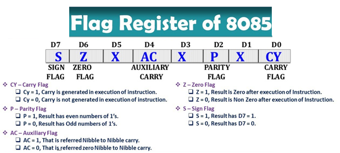
 Carry flag − This flag indicates an overflow condition for arithmetic operations. 


 Auxiliary flag − When an operation is performed at ALU, it results in a carry/barrow from lower nibble (i.e. D0 – D3) to upper nibble (i.e. D4 – D7), then this flag is set, i.e. carry given by D3 bit to D4 is AF flag. The processor uses this flag to perform binary to BCD conversion. 


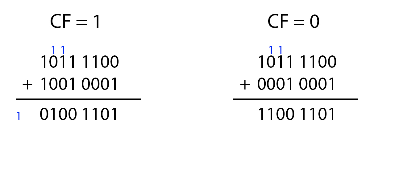
 Parity flag − This flag is used to indicate the parity of the result, i.e. when the lower order 8-bits of the result contains even number of 1’s, then the Parity Flag is set. For odd number of 1’s, the Parity Flag is reset. 


 Zero flag − This flag is set to 1 when the result of arithmetic or logical operation is zero else it is set to 0. 

 Sign flag − This flag holds the sign of the result, i.e. when the result of the operation is negative, then the sign flag is set to 1 else set to 0. 

 Overflow flag − This flag represents the result when the system capacity is exceeded. Control Flags Control flags controls the operations of the execution unit. Following is the list of control flags − 

 Trap flag − It is used for single step control and allows the user to execute one instruction at a time for debugging. If it is set, then the program can be run in a single step mode. 

 Interrupt flag − It is an interrupt enable/disable flag, i.e. used to allow/prohibit the interruption of a program. It is set to 1 for interrupt enabled condition and set to 0 for interrupt disabled condition. 

 Direction flag − It is used in string operation. As the name suggests when it is set then string bytes are accessed from the higher memory address to the lower memory address and vice-a-versa. 

General purpose register:

 There are 8 general purpose registers, i.e., AH, AL, BH, BL, CH, CL, DH, and DL. These registers can be used individually to store 8-bit data and can be used in pairs to store 16bit data. The valid register pairs are AH and AL, BH and BL, CH and CL, and DH and DL. It is referred to the AX, BX, CX, and DX respectively.  

 AX register − It is also known as accumulator register. It is used to store operands for arithmetic operations. 

 BX register − It is used as a base register. It is used to store the starting base address of the memory area within the data segment. 

 CX register − It is referred to as counter. It is used in loop instruction to store the loop counter. 

 DX register − This register is used to hold I/O port address for I/O instruction.  


Q2. Explain the various addressing modes of 8086 with suitable example.

Ans : clickπŸ‘‰ Addressing modes of 8086

Types of addressing mode in 8086

  1. Immediate addressing mode: MOV AX,10ABH
  2. Direct addressing mode: MOV AX, [5000H]
  3. Register addressing mode: MOV AX,BX
  4. Register Indirect addressing mode: MOV AX,[BX]
  5. Indexed addressing mode: MOV AX,[SI]
  6. Register relative addressing mode: MOV AX, 50H[BX]
  7. Base plus index addressing mode: MOV AX, [BX] [SI]
  8. Base relative plus index addressing mode: MOV AX,50H[BX][SI]


Q3. Explain the following instructions:

(i) XCHG

(ii) CLD

(iii) AAA

(iv)CMPS

Answer: Click on this πŸ‘‰πŸ“Q3#Notes

Q4. WAP to find the smallest number among a string of 10 data bytes starting from location 2000H: 3000H and store the result in 2000H: 0500H.


For any further updates , Please visit this page on Regular Interval

Images may be subject to copyright

~Pradeep Kumar

Friday, January 13, 2023

UNIT I: Introduction to Basic Microprocessors Questions and Notes

UNIT I: Introduction to Basic Microprocessors: Historical Background, the Harvard and Princeton architecture, The Microprocessor-Based Personal Computer Systems. The Microprocessor 8085, 8088 basics and comparison (Block & Pin diagram only).

syllabus source:

https://csvtu.ac.in/ew/download/b-tech-5th-semester-5/?wpdmdl=14364&refresh=63c10f5a398271673596762

Prerequisite: Study the following Block diagram first to answer the Questions.

1. Block diagram for the Harvard and Princeton architecture.

2. Block Diagram for Microprocessor 8085

3. Pin Diagram for Microprocessor 8085

4. 8085 vs 8088

Questions: Compiled from previous year CSVTU QPs

1. Write the Difference between Harvard & Princeton Architecture.

πŸ‘‰Note: The Von Neumann (a.k.a. Princeton) architecture.


Difference Between Von Neumann and Harvard Architecture

Parameters

Von Neumann Architecture

Harvard Architecture

Definition

The Von Neumann Architecture is an ancient type of computer architecture that follows the concept of a stored-program computer.

Harvard Architecture is a modern type of computer architecture that follows the concept of the relay-based model by Harvard Mark I.

Physical Address

It uses one single physical address for accessing and storing both data and instructions.

It uses two separate physical addresses for storing and accessing both instructions and data.

Buses (Signal Paths)

One common signal path (bus) helps in the transfer of both instruction and data.

It uses separate buses for the transfer of both data and instructions.

Number of Cycles

It requires two clock cycles for executing a single instruction.

It executes any instruction using only one single cycle.

Cost

It is comparatively cheaper in cost than Harvard Architecture.

It is comparatively more expensive than the Von Neumann Architecture.

Access to CPU

The CPU is not able to read/write data and access instructions at the same time.

The CPU can easily read/write data as well as access the instructions at any given time.

Uses

This method comes to play in the case of small computers and personal computers.

This architecture is best for signal processing as well as microcontrollers.

Requirement of Hardware

As compared to Harvard Architecture, Von Neumann Architecture requires lesser architecture. It is because it only needs to reach one common memory.

This one requires more hardware. It is because it requires separate sets of data as well as address buses for individual memory.

Requirement of Space

This architecture basically requires less space.

This architecture comparatively requires more space.

Usage of Space

This architecture does not waste any space. It is because the instruction memory can utilize the left space of the data memory. It can also happen vice-versa.

This type of architecture can result in space wastage. It is because the instruction memory cannot utilize the leftover space in the data memory. It also cannot happen vice-versa.

Execution Speed

The speed of execution of the Von Neumann Architecture is comparatively slower. It is because it is not capable of fetching the instructions and data both at the same time.

The overall speed of execution of Harvard Architecture is comparatively faster. It is because the processor, in this case, is capable of fetching both instructions and data at the very same time.

Controlling

The process of controlling becomes comparatively simpler with this architecture. It is because it fetches either instructions or data at any given time.

The process of controlling becomes comparatively complex with this architecture. It is because it basically fetches both instructions and data simultaneously at the very same time.

2. Draw & Explain the Internal Architecture of 8085 in brief.

or
Explain the internal architecture of 8085 
microprocessor with basic functional block.

Ans: 


3. Give Classification of Pin in 8085 with neat Diagram

Ans: Pin Diagram of 8085:

The pins of a 8085 microprocessor can be classified into seven groups:

Address bus: A15-A8

Data bus: AD7-AD0, it carries the least significant 8-bit address and data bus.

Control and status signals: Control signals are RD, WR & ALE, Status signals are IO/M, S0 & S1

Power supply: VCC & VSS.

Clock signals: 3 clock signals, i.e. X1, X2, CLK OUT

Interrupts & externally initiated signals: There are 5 interrupt signals, i.e. TRAP, RST 7.5, RST 6.5, RST 5.5, and INTR.

HOLD , HLDA (HOLD Acknowledge).

Serial I/O signals: SID and SOD. 

Classification of Signals:


4. Give Comparison between Microprocessor 8085 and 8086.

Ans. Also refer the Architecture and pin diagram of 8085 and 8086.

Comparison between 8085 & 8086 Microprocessor 

  Size − 8085 is 8-bit microprocessor, whereas 8086 is 16-bit microprocessor. 

 Address Bus − 8085 has 16-bit address bus while 8086 has 20-bit address bus. 

 Memory − 8085 can access up to 64Kb, whereas 8086 can access up to 1 Mb of memory. 

 Instruction − 8085 doesn’t have an instruction queue, whereas 8086 has an instruction queue. 

 Pipelining − 8085 doesn’t support a pipelined architecture while 8086 supports a pipelined architecture. 

 I/O − 8085 can address 2^8 = 256 I/O's, whereas 8086 can access 2^16 = 65,536 I/O's. 

 Cost − The cost of 8085 is low whereas that of 8086 is high.

5. Give Pin Diagram of 8086 with neat label of pin Diagram.

o   8086 Microprocessor is an enhanced version of 8085 Microprocessor 

    Designed by Intel in 1976.It is a 16-bit Microprocessor, 20 address lines 16 data lines, Provides up to 1MB storage. It consists of powerful instruction set, which provides operations like multiplication and division easily.


6. Draw the Internal Architecture of 8086 and Explain the function of each unit of the same in brief.

Ans: 

The internal architecture of Intel 8086 is divided into 2 units: 

The Bus Interface Unit (BIU), and The Execution Unit (EU). 


8086 Architecture

Memory segmentation: 

  • In order to increase execution speed and fetching speed, 8086 segments the memory. 
  • Its 20-bit address bus can address 1MB of memory, it segments it into 16 64kB segments. 
  • 8086 works only with four 64KB segments within the whole 1MB memory.

7. Explain the functions of the following signals of 8085.

(1)  ALE

(ii)  IO/M

(iii) RD

(iv) READY

(v) TRAP

(vi) INTR & INTA

(vii) HOLD & HLDA

(viii) RESET IN

Ans: Refer pins of 8085

Q. 8085 vs 8086 vs 8088


The architecture of 8088 is same as 8086 architecture, but there are two changes. The 8088 has a 4-byte instruction queue in place of 6-byte instruction queue in 8086 and the data bus of 8088 is 8-bit.
There is no concept of even-address bank and odd-address bank of memory in 8088.
As the data bus is 8-bit, the 8088 can access only a byte at a time. Therefore, the speed of operation of 8088 will be reduced as compared to 8086, though internal data bus of 8088 is 16 bits and it can process the 16-bit data internally. 


DIFFERENCES:

808580868088
8085 is an 8 bit microprocessor.8086 is a 16 bit microprocessor.8088 is a 16 bit microprocessor.
It has 8 bit data bus.πŸ˜ƒIt has 16 bit data bus.πŸ˜ƒIt has 8 bit data bus.
It has 8 bit ALU.It has 16 bit ALU.It has 16 bit ALU.
8085 does not require memory banking as it has an 8 bit data bus.8086 requires memory banking to transfer 16 bit data at a time.

8088 does not require memory banking as it has an 8 bit data bus.
8085 performs slower memory operations as it can transfer only 8 bits in one cycle.8086 performs faster memory operations as it can transfer 16 bits in one cycle.8088 performs slower memory operations as it can transfer only 8 bits in one cycle.
8085 does not support pipeline architecture.8086 supports pipeline architecture.8088 supports pipeline architecture.
8085 has no pre-fetch queue as it does not support pipelining.8086 has a 6 byte pre-fetch queue for pipelining.πŸ˜ƒ8088 has a 4 byte pre-fetch queue for pipelining.
8085 has an IO/ pin to differentiate between memory and I/O operations.8086 has an M/ pin to differentiate between memory and I/O operations.8088 has an IO/ pin to differentiate between memory and I/O operations.
8085 has no pre-fetchqueue.8086 BIU will fetch new bytes into the pipelining queue when 2 bytes of the queue are empty.8088 BIU will fetch a new byte into the pipelining queue when 1 byte of the queue is empty.
8085 has 5 flags.8086 has 9 flags.8088 has 9 flags.


πŸ˜ƒFor further updates do visit this page regularly.

Thank you all

Images may be subject to copyright

~Pradeep Kumar