
MEMORY SYSTEMS:
The memory hierarchy system consists of all storage devices contained in a computer system from the slow Auxiliary Memory to fast Main Memory and to smaller Cache memory.
Auxiliary memory access time is generally 1000 times that of the main memory, hence it is at the bottom of the hierarchy.

The Goal:👨 illusion of large, fast, cheap memory
• Fact: Large memories are slow, fast memories are small
• How do we create a memory that is large, cheap and fast (most of the time)?
– Hierarchy
– Parallelism
so,
– Present the user with as much memory as is available in the cheapest technology.
– Provide access at the speed offered by the fastest technology.
How is the hierarchy managed?
• Registers <-------> Memory – by compiler (programmer?)
• cache <-------> memory – by the hardware
• memory <--------> disks – by the hardware and operating system (virtual memory) – by the programmer (files)
• Virtual memory – Virtual layer between application address space to physical memory – Not part of the physical memory hierarchy
Memory Technology
*Random Access: – "Random" is good: access time is the same for all locations
– DRAM: Dynamic Random Access Memory
• High density, low power, cheap, slow
• Dynamic: need to be refreshed regularly
• Main Memory is DRAM
See My Lecture/ VIDEO : Click 👉🎬 or Directly click on the Video below:
– SRAM: Static Random Access Memory
• Cache uses SRAM : Static Random Access Memory – No refresh
• Low density, high power, expensive, fast
• Static: content will last forever (until lose power)
Example:

* "Non-so-random" Access Technology: – Access time varies from location to location and from time to time
– Examples: Disk, CDROM
* Sequential Access Technology: access time linear in location (e.g., Tape)
So,
• DRAM is slow but cheap and dense: – Good choice for presenting the user with a BIG memory system
• SRAM is fast but expensive and not very dense: – Good choice for providing the user FAST access time.
Increasing Bandwidth - Interleaving : Refer Question#
Disk Storage
• Nonvolatile, rotating magnetic storage:

Magnetic Disks
- Traditional magnetic disks have the following basic structure:
- One or more platters in the form of disks covered with magnetic media. Hard disk platters are made of rigid metal, while "floppy" disks are made of more flexible plastic.
- Each platter has two working surfaces. Older hard disk drives would sometimes not use the very top or bottom surface of a stack of platters, as these surfaces were more susceptible to potential damage.
- Each working surface is divided into a number of concentric rings called tracks. The collection of all tracks that are the same distance from the edge of the platter, ( i.e. all tracks immediately above one another in the following diagram ) is called a cylinder.
- Each track is further divided into sectors, traditionally containing 512 bytes of data each, although some modern disks occasionally use larger sector sizes. ( Sectors also include a header and a trailer, including checksum information among other things. Larger sector sizes reduce the fraction of the disk consumed by headers and trailers, but increase internal fragmentation and the amount of disk that must be marked bad in the case of errors. )
- The data on a hard drive is read by read-write heads. The standard configuration ( shown below ) uses one head per surface, each on a separate arm, and controlled by a common arm assembly which moves all heads simultaneously from one cylinder to another. ( Other configurations, including independent read-write heads, may speed up disk access, but involve serious technical difficulties. )
- The storage capacity of a traditional disk drive is equal to the number of heads ( i.e. the number of working surfaces ), times the number of tracks per surface, times the number of sectors per track, times the number of bytes per sector. A particular physical block of data is specified by providing the head-sector-cylinder number at which it is located.

****************************************************
Questions and Answers ( As per previous year CSVTU QP):
1. Explain Memory Hierarchy , give details of each levels in brief.
Ans:


Levels of memory:
• Level 0 or Register – It is a type of memory in which data is stored and accepted that are immediately stored in CPU. Most commonly used register is accumulator, Program counter, address register etc.
• Level 1 or Cache memory – It is the fastest memory which has faster access time where data is temporarily stored for faster access.
• Level 2 or Main Memory – It is memory on which computer works currently. It is small in size and once power is off data no longer stays in this memory.
• Level 3 or Secondary Memory – It is external memory which is not as fast as main memory but data stays permanently in this memory.
2. What is Virtual memory in Computer System? Give Details of Paging Mechanism. How it is different from Main memory.
Ans: See my Class notes: Click👉 Paging Mechanism
OR
Virtual memory is a memory management technique where secondary memory can be used as if it were a part of the main memory.
Virtual memory is a valuable concept in computer architecture that allows you to run large, sophisticated programs on a computer even if it has a relatively small amount of RAM. A computer with virtual memory artfully juggles the conflicting demands of multiple programs within a fixed amount of physical memory.
Virtual memory is a common technique used in a computer's operating system (OS).
How does virtual storage work?
This memory system uses both the computer's software and hardware to work. It transfers processes between the computer's RAM and hard disk by copying any files from RAM that aren't currently in use and moving them to the hard disk.
Virtual storage management:
Computers can handle virtual storage through segmenting and paging. Below is an explanation of the Paging Mechanism.
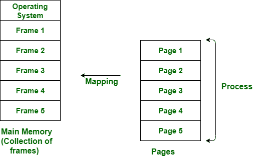
Paging Mechanism:
Paging is a Memory management method.
The process of retrieving processes in the form of pages from the secondary storage into the main memory is known as paging.
In paging, the physical memory is divided into fixed-size blocks called page frames, which are the same size as the pages used by the process. The process’s logical address space is also divided into fixed-size blocks called pages, which are the same size as the page frames.
Now we usually divide the Main Memory in to Frames of equal sizes. And in return each of the Frame consists of equal number of words.
Important Point to be noted is that Page Size = Frame Size.
Let us assume 2 processes, P1 and P2, contains 4 pages each. Each page size is 1 KB. The main memory contains 8 frame of 1 KB each. The OS resides in the first two partitions. In the third partition, 1st page of P1 is stored and the other frames are also shown as filled with the different pages of processes in the main memory.
The page tables of both the pages are 1 KB size each and therefore they can be fit in one frame each. The page tables of both the processes contain various information that is also shown in the image.
The CPU contains a register which contains the base address of page table that is 5 in the case of P1 and 7 in the case of P2. This page table base address will be added to the page number of the Logical address when it comes to accessing the actual corresponding entry.

A Translation look aside buffer can be defined as a memory cache which can be used to reduce the time taken to access the page table again and again.
It is a memory cache which is closer to the CPU and the time taken by CPU to access TLB is lesser then that taken to access main memory.

3. A Two way Set Associative Cache Memory uses a Block of Size 128 bytes with Total Cache Size 1MB. Byte . Addressable Main Memory Size is given as 256 MB.
Give the Physical Address Splits in bits.
Ans: See my Class notes :
click 👉 Types of Cache mapping Theory with Solved Numerical
or
First lets see the theory behind it:
In OS we have two kind of addresses:
Virtual/Logical Address, and Physical Address.
Physical Address:
As explained above that CPU generates addresses of all the processes in the main memory relative to zero i.e., CPU produces address starting from 0.Now the addresses generated by are no way real because if those addresses were valid then all processes would begin from zero and rest spaces in Main Memory would be memory. Thus the addresses generated by CPU should be some way mapped to real (physical address) of the Main Memory. This is done by MMU (Memory Management unit).

he smallest addressable unit in memory is called word. It means the smallest unit which can specifically identified using address bits.
The Address Space of Virtual Address is divided into 2 parts: Page Number, and Page OFFset.
Similarly, the Address Space of Physical Address is divided into 2 parts: Frame Number, and Frame OFFset.
Let Virtual Address has n bits and Physical Address has m bits.
Page Size = Frame Size = k bits
(as page size = Frame size as mentioned above).
Number of Pages = 2(n-k) pagesNumber of Frames = 2(m-k) Frames


5. Give all Information required to construct Cache Memory.
Ans:
Cache Memory
Cache Memory is a special very high-speed memory. It is used to speed up and synchronizing with high-speed CPU.
Cache Performance:
When the processor needs to read or write a location in main memory, it first checks for a corresponding entry in the cache.
• If the processor finds that the memory location is in the cache, a cache hit has occurred and data is read from cache
• If the processor does not find the memory location in the cache, a cache miss has occurred. For a cache miss, the cache allocates a new entry and copies in data from main memory, then the request is fulfilled from the contents of the cache.
The performance of cache memory is frequently measured in terms of a quantity called Hit ratio.
Hit ratio = hit / (hit + miss) = no. of hits/total accesses
- Direct Mapping –
Maps each block of main memory into only one possible cache line. If a line is previously taken up by a memory block and a new block needs to be loaded, the old block is trashed. An address space is split into two parts index field and a tag field. The cache is used to store the tag field whereas the rest is stored in the main memory. - Associative Mapping –
A block of main memory can map to any line of the cache that is freely available at that moment. The word offset bits are used to identify which word in the block is needed, all of the remaining bits become Tag. - Set-Associative Mapping –
Cache lines are grouped into sets where each set contains k number of lines and a particular block of main memory can map to only one particular set of the cache. However, within that set, the memory block can map to any freely available cache line.
Cache Mapping:
- There are three different types of mapping used for the purpose of cache memory which is as follows: Direct mapping, Associative mapping, and Set-Associative mapping.
Note: Translation Lookaside Buffer (i.e. TLB) is required only if Virtual Memory is used by a processor. In short, TLB speeds up the translation of virtual address to a physical address by storing page-table in faster memory. In fact, TLB also sits between the CPU and Main memory.

What is Direct Mapping?
(source:https://byjus.com/gate/direct-mapping-notes/)
In the case of direct mapping, a certain block of main memory would be able to map to only a particular line of cache.
Physical Address Division
The physical address, in the case of direct mapping, is divided as follows:


What is Fully Associative Mapping?
“Every memory block can be mapped to any cache line.”
The fully associative mapping helps us resolve the issue related to conflict misses. It means that any block of the main memory can easily come in a line of cache memory. Here, for instance, B0 can easily come in L1, L2, L3, and L4. Also, the case would be similar for all the other blocks. This way, the chances of a cache hit increase a lot.
Now, let us assume that there is a RAM (Main Memory) size of 128 Words along with a Cache size of 16 Words. Here, the Cache and the Main Memory are divided into Lines and blocks, respectively. Every block Line is of the size 4- words. It is shown in the diagram given as follows:

Physical Address
Since the main memory has a size of 128 words, a total of 7 bits would be used for representing the main memory. Thus, the Physical address would be 7 bits in size. Given below is an example of the fully associative mapping of W24 of the B6.

What is K-way Set Associative Mapping?
The K-way set associative mapping is like a mix of fully associative and direct mapping. Here,
- The total number of sets = The total number of lines/K
- K refers to the K-way set associative
- K= 23 for a 2-way set associative
- The total number of sets = 4/2 or 2 sets (S1, S0)

Physical Address
In case a cache has 4 lines, and we consider a 2-way set associative, then:

6. What is Memory Interleaving?
Ans:
See my Class notes : click 👉 Memory Interleaving
or
Prerequisite – see Q#2.
Abstraction is one of the most important aspects of computing. It is a widely implemented Practice in the Computational field.
Memory Interleaving is less or More an Abstraction technique. Though it’s a bit different from Abstraction.
It is a Technique that divides memory into a number of modules such that Successive words in the address space are placed in the Different modules.
***************************************************************************
Thank you all
~pradeep
Educational Purpose Only: The information provided on this blog is for general informational and educational purposes only. All content, including text, graphics, images, and other material contained on this blog, is intended to be a resource for learning and should not be considered as professional advice.
No Professional Advice: The content on this blog does not constitute professional advice, and you should not rely on it as a substitute for professional consultation, diagnosis, or treatment. Always seek the advice of a qualified professional with any questions you may have regarding a specific issue.
Accuracy of Information: While I strive to provide accurate and up-to-date information, I make no representations or warranties of any kind, express or implied, about the completeness, accuracy, reliability, suitability, or availability with respect to the blog or the information, products, services, or related graphics contained on the blog for any purpose. Any reliance you place on such information is therefore strictly at your own risk.
External Links: This blog may contain links to external websites that are not provided or maintained by or in any way affiliated with me. Please note that I do not guarantee the accuracy, relevance, timeliness, or completeness of any information on these external websites.
Personal Responsibility: Readers of this blog are encouraged to do their own research and consult with a professional before making any decisions based on the information provided. I am not responsible for any loss, injury, or damage that may result from the use of the information contained on this blog.
Contact: If you have any questions or concerns regarding this disclaimer, please feel free to contact me at my email: pradeep14335@gmail.com


